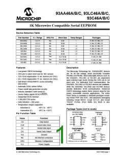
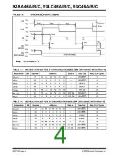
93AA46A/B/C, 93LC46A/B/C, 93C46A/B/C
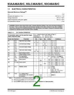
1.0
ELECTRICAL CHARACTERISTICS
(†)
Absolute Maximum Ratings
VCC.............................................................................................................................................................................7.0V
All inputs and outputs w.r.t. VSS ......................................................................................................... -0.6V to VCC +1.0V
Storage temperature ...............................................................................................................................-65°C to +150°C
Ambient temperature with power applied................................................................................................-40°C to +125°C
ESD protection on all pins ......................................................................................................................................................≥ 4 kV
† NOTICE: Stresses above those listed under “Absolute Maximum Ratings” may cause permanent damage to
the device. This is a stress rating only and functional operation of the device at those or any other conditions
above those indicated in the operational listings of this specification is not implied. Exposure to maximum rating
conditions for extended periods may affect device reliability.
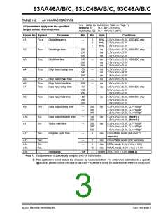
TABLE 1-1:
DC CHARACTERISTICS
VCC = range by device (see Table on Page 1)
Industrial (I): TA = -40°C to +85°C
Automotive (E): TA = -40°C to +125°C
All parameters apply over the specified ranges
unless otherwise noted.
Param. No. Symbol
Parameter
Min
Typ
Max
Units
Conditions
VCC ≥ 2.7V
D1
D2
D3
D4
VIH1
VIH2
High-level input voltage
2.0
0.7 VCC
—
—
VCC +1
VCC +1
V
V
VCC < 2.7V
VIL1
VIL2
Low-level input voltage
Low-level output voltage
High-level output voltage
-0.3
-0.3
—
—
0.8
0.2 VCC
V
V
VCC ≥ 2.7V
VCC < 2.7V
VOL1
VOL2
—
—
—
—
0.4
0.2
V
V
IOL = 2.1 mA, VCC = 4.5V
IOL = 100 µA, VCC = 2.5V
VOH1
VOH2
2.4
VCC - 0.2
—
—
—
—
V
V
IOH = -400 µA, VCC = 4.5V
IOH = -100 µA, VCC = 2.5V
D5
D6
D7
ILI
Input leakage current
Output leakage current
—
—
—
—
—
—
±1
±1
7
µA VIN = VSS to VCC
µA VOUT = VSS to VCC
ILO
CIN,
Pin capacitance
pF VIN/VOUT = 0V (Note 1)
COUT
(all inputs/outputs)
TA = 25°C, FCLK = 1 MHz
D8
D9
ICC
write
Write current
—
—
—
500
2
—
mA FCLK = 3 MHz, VCC = 5.5V
µA FCLK = 2 MHz, VCC = 2.5V
ICC read Read current
—
—
—
—
—
100
1
500
—
mA FCLK = 3 MHz, VCC = 5.5V
µA FCLK = 2 MHz, VCC = 3.0V
µA FCLK = 2 MHz, VCC = 2.5V
D10
D11
ICCS
Standby current
—
—
—
—
1
5
µA I-Temp
µA E-Temp
CLK = CS = 0V
ORG = DI = VSS or VCC
(Note 2) (NOTE 3)
VPOR
VCC voltage detect
93AA46A/B/C, 93LC46A/B/C
93C46A/B/C
—
—
1.5V
3.8V
—
—
V
V
(Note 1)
Note 1: This parameter is periodically sampled and not 100% tested.
2: ORG pin not available on ‘A’ or ‘B’ versions.
3: READY/BUSY status must be cleared from DO, see Section 3.4 "Data Out (DO)".
DS21749D-page 2
2003 Microchip Technology Inc.

 MICROCHIP [ MICROCHIP ]