93AA46A/B/C, 93LC46A/B/C, 93C46A/B/C
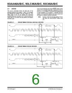
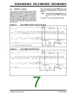
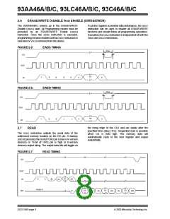
2.3
Data Protection
2.0
FUNCTIONAL DESCRIPTION
All modes of operation are inhibited when VCC is below
a typical voltage of 1.5V for '93AA' and '93LC' devices
or 3.8V for '93C' devices.
When the ORG* pin is connected to VCC, the (x16)
organization is selected. When it is connected to
ground, the (x8) organization is selected. Instructions,
addresses and write data are clocked into the DI pin on
the rising edge of the clock (CLK). The DO pin is
normally held in a HIGH-Z state except when reading
data from the device, or when checking the READY/
BUSY status during a programming operation. The
READY/BUSY status can be verified during an Erase/
Write operation by polling the DO pin; DO low indicates
that programming is still in progress, while DO high
indicates the device is ready. DO will enter the HIGH-Z
state on the falling edge of CS.
The EWEN and EWDS commands give additional
protection against accidentally programming during
normal operation.
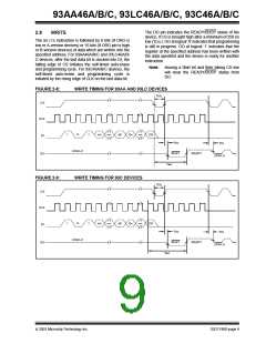
Note: For added protection, an EWDS command
should be performed after every write
operation.
After power-up, the device is automatically in the
EWDS mode. Therefore, an EWENinstruction must be
performed before the initial ERASEor WRITEinstruction
can be executed.
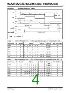
2.1
Start Condition
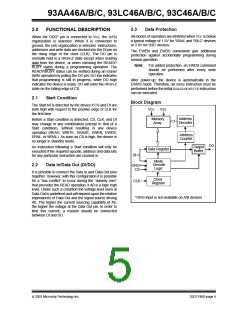
Block Diagram
The Start bit is detected by the device if CS and DI are
both high with respect to the positive edge of CLK for
the first time.
VCC
VSS
Address
Decoder
Memory
Array
Before a Start condition is detected, CS, CLK, and DI
may change in any combination (except to that of a
Start condition), without resulting in any device
operation (READ, WRITE, ERASE, EWEN, EWDS,
ERAL, or WRAL). As soon as CS is high, the device is
no longer in Standby mode.
Address
Counter
DO
An instruction following a Start condition will only be
executed if the required opcode, address and data bits
for any particular instruction are clocked in.
Output
Buffer
Data Register
DI
Mode
Decode
Logic
2.2
Data In/Data Out (DI/DO)
ORG*
CS
It is possible to connect the Data In and Data Out pins
together. However, with this configuration it is possible
for a “bus conflict” to occur during the “dummy zero”
that precedes the READ operation, if A0 is a logic high
level. Under such a condition the voltage level seen at
Data Out is undefined and will depend upon the relative
impedances of Data Out and the signal source driving
A0. The higher the current sourcing capability of A0,
the higher the voltage at the Data Out pin. In order to
limit this current, a resistor should be connected
between DI and DO.
Clock
Register
CLK
*ORG input is not available on A/B devices
2003 Microchip Technology Inc.
DS21749D-page 5

 MICROCHIP [ MICROCHIP ]