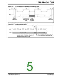
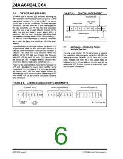
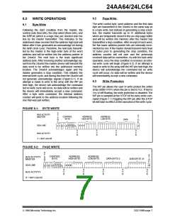
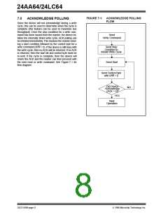
24AA64/24LC64
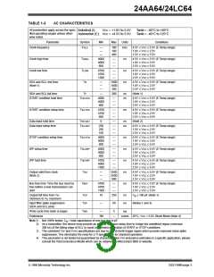
TABLE 1-1
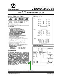
Name
PIN FUNCTION TABLE
Function
1.0
ELECTRICAL
CHARACTERISTICS
1.1
Maximum Ratings*
A0,A1,A2 User Configurable Chip Selects
VSS
SDA
SCL
WP
Ground
Vcc .................................................................................................7.0V
All inputs and outputs w.r.t. Vss...............................-0.6V to Vcc +1.0V
Storage temperature ................................................... -65˚C to +150˚C
Ambient temp. with power applied............................... -65˚C to +125˚C
Soldering temperature of leads (10 seconds)........................... +300˚C
ESD protection on all pins...........................................................≥ 4 kV
Serial Data
Serial Clock
Write Protect Input
*Notice: Stresses above those listed under “Maximum Ratings” may
cause permanent damage to the device.This is a stress rating only and
functional operation of the device at those or any other conditions
above those indicated in the operational listings of this specification is
not implied. Exposure to maximum rating conditions for extended peri-
ods may affect device reliability.
VCC
+1.8 to 5.5V (24AA64)
+2.5 to 5.5V (24LC64)
TABLE 1-2
DC CHARACTERISTICS
All parameters apply across the
recommended operating ranges
unless otherwise noted.
Industrial (I):
Automotive (E): VCC = 4.5V to 5.5V
VCC = +1.8V to 5.5V
Tamb = -40°C to +85°C
Tamb = -40°C to 125°C
Parameter
Symbol
Min
Max
Units
Conditions
A0, A1, A2,
SCL, SDA, and WP pins:
High level input voltage
Low level input voltage
VIH
VIL
0.7 VCC
—
—
V
V
V
V
0.3 VCC
0.2 VCC
—
VCC ≥ 2.5V
VCC < 2.5V
VCC > 2.5V (Note)
Hysteresis of Schmitt Trigger
inputs (SDA, SCL pins)
Low level output voltage
VHYS
VOL
ILI
0.05 VCC
—
0.40
10
V
IOL = 3.0 mA @ VCC = 4.5V
IOL = 2.1 mA @ VCC = 2.5V
VIN = Vss to VCC, WP = VSS
VIN = Vss or VCC, WP = VCC
VOUT = Vss to VCC
Input leakage current
-10
µA
Output leakage current
Pin capacitance
ILO
CIN, COUT
-10
—
10
10
µA
pF
VCC = 5.0V (Note)
(all inputs/outputs)
Tamb = 25˚C, f = 1 MHz
c
Operating current
ICC Write
ICC Read
ICCS
—
—
—
3
400
1
mA
µA
µA
VCC = 5.5V
VCC = 5.5V, SCL = 400 kHz
SCL = SDA = VCC = 5.5V
A0, A1, A2, WP = VSS
Standby current
Note: This parameter is periodically sampled and not 100% tested.
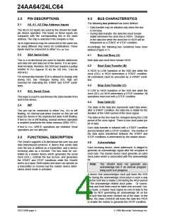
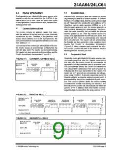
FIGURE 1-1: BUS TIMING DATA
THIGH
VHYS
TF
TR
SCL
TSU:STA
TLOW
THD:DAT
TSU:DAT
TSU:STO
SDA
IN
THD:STA
TSP
TBUF
TAA
SDA
OUT
(protected)
THD:WP
WP
TSU:WP
(unprotected)
DS21189B-page 2
1998 Microchip Technology Inc.

 MICROCHIP [ MICROCHIP ]