24AA64/24LC64
6.2
Page Write
6.0
WRITE OPERATIONS
The write control byte, word address and the first data
byte are transmitted to the 24xx64 in the same way as
in a byte write. But instead of generating a stop condi-
tion, the master transmits up to 31 additional bytes
which are temporarily stored in the on-chip page buffer
and will be written into memory after the master has
transmitted a stop condition. After receipt of each word,
the five lower address pointer bits are internally incre-
mented by one. If the master should transmit more than
32 bytes prior to generating the stop condition, the
address counter will roll over and the previously
received data will be overwritten. As with the byte write
operation, once the stop condition is received, an inter-
nal write cycle will begin (Figure 6-2). If an attempt is
made to write to the array with the WP pin held high, the
device will acknowledge the command but no write
cycle will occur, no data will be written and the device
will immediately accept a new command.
6.1
Byte Write
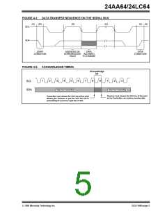
Following the start condition from the master, the
control code (four bits), the chip select (three bits), and
the R/W bit (which is a logic low) are clocked onto the
bus by the master transmitter. This indicates to the
addressed slave receiver that the address high byte will
follow after it has generated an acknowledge bit during
the ninth clock cycle. Therefore, the next byte transmit-
ted by the master is the high-order byte of the word
address and will be written into the address pointer of
the 24xx64. The next byte is the least significant
address byte. After receiving another acknowledge sig-
nal from the 24xx64 the master device will transmit the
data word to be written into the addressed memory
location. The 24xx64 acknowledges again and the
master generates a stop condition. This initiates the
internal write cycle, and during this time the 24xx64 will
not generate acknowledge signals (Figure 6-1). If an
attempt is made to write to the array with the WP pin
held high, the device will acknowledge the command
but no write cycle will occur, no data will be written and
the device will immediately accept a new command.
After a byte write command, the internal address
counter will point to the address location following the
one that was just written.
6.3
Write Protection
The WP pin allows the user to write protect the entire
array (0000-1FFF) when the pin is tied to Vcc. If tied to
VSS or left floating, the write protection is disabled.The
WP pin is sampled at the STOP bit for every write com-
mand (Figure 1-1) Toggling the WP pin after the STOP
bit will have no effect on the execution of the write cycle.
FIGURE 6-1: BYTE WRITE
S
BUS ACTIVITY
T
S
T
O
P
CONTROL
BYTE
ADDRESS
HIGH BYTE
ADDRESS
LOW BYTE
MASTER
A
R
T
DATA
A A A
2 1 0
SDA LINE
X X X
S 1 0 1 0
0
P
A
C
K
A
C
K
A
C
K
A
C
K
BUS ACTIVITY
X = don’t care bit
FIGURE 6-2: PAGE WRITE
S
T
A
R
T
S
T
O
P
CONTROL
BYTE
ADDRESS
HIGH BYTE
ADDRESS
LOW BYTE
BUS ACTIVITY
MASTER
DATA BYTE 0
DATA BYTE 31
A A A
2 1 0
SDA LINE
X X X
P
S 1 0 1 0
0
A
C
K
A
C
K
A
C
K
A
C
K
A
C
K
BUS ACTIVITY
X = don’t care bit
1998 Microchip Technology Inc.
DS21189B-page 7

 MICROCHIP [ MICROCHIP ]