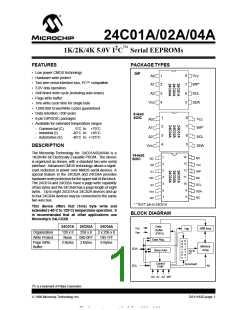
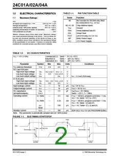
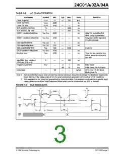
24C01A/02A/04A
4.0
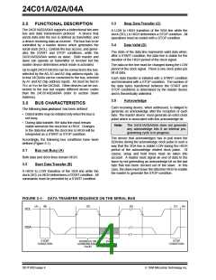
SLAVE ADDRESS
6.0
PAGE PROGRAM MODE
The chip address inputs A0, A1 and A2 of each 24C01A/
02A/04A must be externally connected to either VCC or
ground (VSS), assigning to each 24C01A/02A/04A a
unique address. A0 is not used on the 24C04A and
must be connected to either VCC or VSS. Up to eight
24C01A or 24C02A devices and up to four 24C04A
devices may be connected to the bus. Chip selection is
then accomplished through software by setting the bits
A0, A1 and A2 of the slave address to the corresponding
hard-wired logic levels of the selected 24C01A/02A/04A.
After generating a START condition, the bus master
transmits the slave address consisting of a 4-bit device
code (1010) for the 24C01A/02A/04A, followed by the
chip address bits A0, A1 and A2. In the 24C04A, the
seventh bit of that byte (A0) is used to select the upper
block (addresses 100—1FF) or the lower block
(addresses 000—0FF) of the array.
To program the 24C01A/02A/04A, the master sends
addresses and data to the 24C01A/02A/04A which is
the slave (Figure 6-1 and Figure 6-2). This is done by
supplying a START condition followed by the 4-bit
device code, the 3-bit slave address, and the R/W bit
which is defined as a logic LOW for a write. This indi-
cates to the addressed slave that a word address will
follow so the slave outputs the acknowledge pulse to
the master during the ninth clock pulse. When the word
address is received by the 24C01A/02A/04A, it places
it in the lower 8 bits of the address pointer defining
which memory location is to be written. (The A0 bit
transmitted with the slave address is the ninth bit of the
address pointer for the 24C04A). The 24C01A/02A/04A
will generate an acknowledge after every 8-bits
received and store them consecutively in a RAM buffer
until a STOP condition is detected. This STOP condi-
tion initiates the internal programming cycle. The RAM
buffer is 2 bytes for the 24C01A/02A and 8 bytes for the
24C04A. If more than 2 bytes are transmitted by the
master to the 24C01A/02A, the device will not acknowl-
edge the data transfer and the sequence will be
aborted. If more than 8 bytes are transmitted by the
master to the 24C04A, it will roll over and overwrite the
data beginning with the first received byte. This does
not affect erase/write cycles of the EEPROM array and
is accomplished as a result of only allowing the address
registers bottom 3 bits to increment while the upper 5
bits remain unchanged.
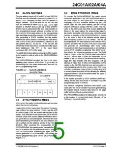
The eighth bit of slave address determines if the master
device wants to read or write to the 24C01A/02A/04A
(Figure 4-1).
The 24C01A/02A/04A monitors the bus for its corre-
sponding slave address all the time. It generates an
acknowledge bit if the slave address was true and it is
not in a programming mode.
FIGURE 4-1: SLAVE ADDRESS
ALLOCATION
START
READ/WRITE
If the master generates a STOP condition after trans-
mitting the first data word (Point ‘P’ on Figure 6-1), byte
programming mode is entered.
SLAVE ADDRESS
R/W
A
The internal, completely self-timed PROGRAM cycle
starts after the STOP condition has been generated by
the master and all received data bytes in the page
buffer will be written in a serial manner.
1
0
1
0
A2
A1
A0
The PROGRAM cycle takes N milliseconds, whereby N
is the number of received data bytes (N max = 8 for
24C04A, 2 for 24C01A/02A).
5.0
BYTE PROGRAM MODE
In this mode, the master sends addresses and one data
byte to the 24C01A/02A/04A.
Following the START signal from the master, the device
code (4-bits), the slave address (3-bits), and the R/W
bit, which is logic LOW, are placed onto the bus by the
master. This indicates to the addressed 24C01A/02A/
04A that a byte with a word address will follow after it
has generated an acknowledge bit. Therefore the next
byte transmitted by the master is the word address and
will be written into the address pointer of the 24C01A/
02A/04A. After receiving the acknowledge of the
24C01A/02A/04A, the master device transmits the data
word to be written into the addressed memory location.
The 24C01A/02A/04A acknowledges again and the
master generates a STOP condition. This initiates the
internal programming cycle of the 24C01A/02A/04A
(Figure 6-1).
1996 Microchip Technology Inc.
DS11183D-page 5

 MICROCHIP [ MICROCHIP ]