24C01A/02A/04A
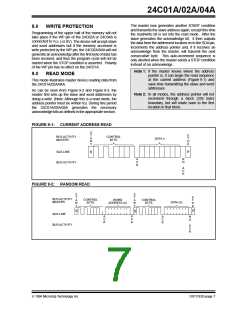
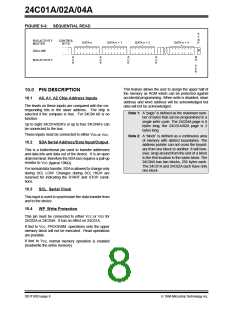
FIGURE 9-3: SEQUENTIAL READ
S
T
O
P
BUS ACTIVITY
MASTER
CONTROL
BYTE
DATA n
DATA n + 1
DATA n + 2
DATA n + X
SDA LINE
P
A
C
K
A
C
K
A
C
K
A
C
K
N
O
BUS ACTIVITY
A
C
K
This feature allows the user to assign the upper half of
the memory as ROM which can be protected against
accidental programming. When write is disabled, slave
address and word address will be acknowledged but
data will not be acknowledged.
10.0 PIN DESCRIPTION
10.1
A0, A1, A2 Chip Address Inputs
The levels on these inputs are compared with the cor-
responding bits in the slave address. The chip is
selected if the compare is true. For 24C04 A0 is no
function.
Note 1: A “page” is defined as the maximum num-
ber of bytes that can be programmed in a
single write cycle. The 24C04A page is 8
bytes long; the 24C01A/02A page is 2
bytes long.
Up to eight 24C01A/02A's or up to four 24C04A's can
be connected to the bus.
These inputs must be connected to either VSS or VCC.
Note 2: A “block” is defined as a continuous area
of memory with distinct boundaries. The
address pointer can not cross the bound-
ary from one block to another. It will how-
ever, wrap around from the end of a block
to the first location in the same block. The
24C04A has two blocks, 256 bytes each.
The 24C01A and 24C02A each have only
one block.
10.2
SDASerialAddress/DataInput/Output
This is a bidirectional pin used to transfer addresses
and data into and data out of the device. It is an open
drain terminal, therefore the SDA bus requires a pull-up
resistor to VCC (typical 10KΩ).
For normal data transfer, SDAis allowed to change only
during SCL LOW. Changes during SCL HIGH are
reserved for indicating the START and STOP condi-
tions.
10.3
SCL Serial Clock
This input is used to synchronize the data transfer from
and to the device.
10.4
WP Write Protection
This pin must be connected to either VCC or VSS for
24C02A or 24C04A. It has no effect on 24C01A.
If tied to VCC, PROGRAM operations onto the upper
memory block will not be executed. Read operations
are possible.
If tied to VSS, normal memory operation is enabled
(read/write the entire memory).
DS11183D-page 8
1996 Microchip Technology Inc.

 MICROCHIP [ MICROCHIP ]