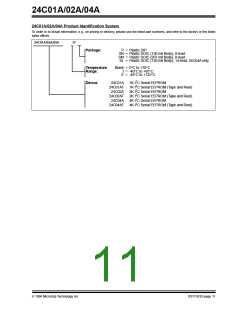
24C01A/02A/04A
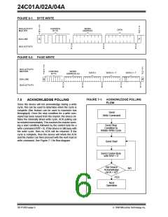
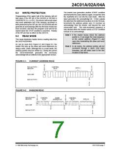
The master now generates another START condition
and transmits the slave address again, except this time
the read/write bit is set into the read mode. After the
slave generates the acknowledge bit, it then outputs
the data from the addressed location on to the SDA pin,
increments the address pointer and, if it receives an
acknowledge from the master, will transmit the next
consecutive byte. This auto-increment sequence is
only aborted when the master sends a STOP condition
instead of an acknowledge.
8.0
WRITE PROTECTION
Programming of the upper half of the memory will not
take place if the WP pin of the 24C02A or 24C04A is
connected to VCC (+5.0V). The device will accept slave
and word addresses but if the memory accessed is
write protected by the WP pin, the 24C02A/04A will not
generate an acknowledge after the first byte of data has
been received, and thus the program cycle will not be
started when the STOP condition is asserted. Polarity
of the WP pin has no effect on the 24C01A.
Note 1: If the master knows where the address
pointer is, it can begin the read sequence
at the current address (Figure 9-1) and
save time transmitting the slave and word
addresses.
9.0
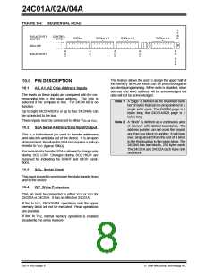
READ MODE
This mode illustrates master device reading data from
the 24C01A/02A/04A.
As can be seen from Figure 9-2 and Figure 9-3, the
master first sets up the slave and word addresses by
doing a write. (Note: Although this is a read mode, the
address pointer must be written to). During this period
the 24C01A/02A/04A generates the necessary
acknowledge bits as defined in the appropriate section.
Note 2: In all modes, the address pointer will not
increment through a block (256 byte)
boundary, but will rotate back to the first
location in that block.
FIGURE 9-1: CURRENT ADDRESS READ
S
T
A
R
T
S
BUS ACTIVITY
MASTER
CONTROL
BYTE
T
DATA n
O
P
SDA LINE
S
P
A
C
K
N
O
BUS ACTIVITY
A
C
K
FIGURE 9-2: RANDOM READ
S
T
A
R
T
S
T
A
R
T
S
T
O
P
BUS ACTIVITY
MASTER
CONTROL
BYTE
WORD
ADDRESS (n)
CONTROL
BYTE
DATA (n)
S
P
S
SDA LINE
A
C
K
A
C
K
A
C
K
N
O
BUS ACTIVITY
A
C
K
1996 Microchip Technology Inc.
DS11183D-page 7

 MICROCHIP [ MICROCHIP ]