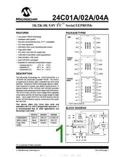
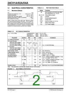
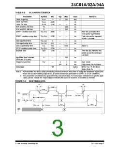
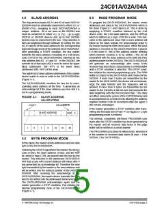
24C01A/02A/04A
3.3
Stop Data Transfer (C)
2.0
FUNCTIONAL DESCRIPTION
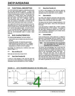
The 24C01A/02A/04A supports a bidirectional two wire
bus and data transmission protocol. A device that
sends data onto the bus is defined as transmitter, and
a device receiving data as receiver. The bus has to be
controlled by a master device which generates the
serial clock (SCL), controls the bus access, and gener-
ates the START and STOP conditions, while the
24C01A/02A/04A works as slave. Both master and
slave can operate as transmitter or receiver but the
master device determines which mode is activated.
A LOW to HIGH transition of the SDA line while the
clock (SCL) is HIGH determines a STOP condition. All
operations must be ended with a STOP condition.
3.4
Data Valid (D)
The state of the data line represents valid data when,
after a START condition, the data line is stable for the
duration of the HIGH period of the clock signal.
The data on the line must be changed during the LOW
period of the clock signal. There is one clock pulse per
bit of data.
Up to eight 24C01/24c02s can be connected to the bus,
selected by the A0, A1 and A2 chip address inputs. Up
to four 24C04As can be connected to the bus, selected
by A1 and A2 chip address inputs. A0 must be tied to
VCC or VSS for the 24C04A. Other devices can be con-
nected to the bus but require different device codes
than the 24C01A/02A/04A (refer to section Slave
Address).
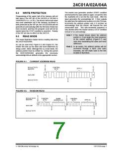
Each data transfer is initiated with a START condition
and terminated with a STOP condition. The number of
the data bytes transferred between the START and
STOP conditions is determined by the master device
and is theoretically unlimited.
3.5
Acknowledge
3.0
BUS CHARACTERISTICS
Each receiving device, when addressed, is obliged to
generate an acknowledge after the reception of each
byte. The master device must generate an extra clock
pulse which is associated with this acknowledge bit.
The following bus protocol has been defined:
• Data transfer may be initiated only when the bus is
not busy.
• During data transfer, the data line must remain
stable whenever the clock line is HIGH. Changes
in the data line while the clock line is HIGH will be
interpreted as a START or STOP condition.
Note: The 24C01A/02A/04A does not generate
any acknowledge bits if an internal pro-
gramming cycle is in progress.
The device that acknowledges has to pull down the
SDA line during the acknowledge clock pulse in such a
way that the SDA line is stable LOW during the HIGH
period of the acknowledge related clock pulse. Of
course, setup and hold times must be taken into
account. A master must signal an end of data to the
slave by not generating an acknowledge bit on the last
byte that has been clocked out of the slave. In this
case, the slave must leave the data line HIGH to enable
the master to generate the STOP condition.
Accordingly, the following bus conditions have been
defined (Figure 3-1).
3.1
Bus not Busy (A)
Both data and clock lines remain HIGH.
3.2
Start Data Transfer (B)
A HIGH to LOW transition of the SDA line while the
clock (SCL) is HIGH determines a START condition. All
commands must be preceded by a START condition.
FIGURE 3-1: DATA TRANSFER SEQUENCE ON THE SERIAL BUS
(A)
(B)
(D)
(D)
(C)
(A)
SCL
SDA
START
CONDITION
STOP
CONDITION
ADDRESS OR
ACKNOWLEDGE
VALID
DATA
ALLOWED
TO CHANGE
DS11183D-page 4
1996 Microchip Technology Inc.

 MICROCHIP [ MICROCHIP ]