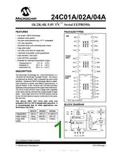
24C01A/02A/04A
TABLE 1-1:
PIN FUNCTION TABLE
Function
1.0
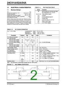
ELECTRICAL CHARACTERISTICS
Name
1.1
Maximum Ratings*
A0
No Function for 24C04A only, Must
be connected to VCC or VSS
VCC...................................................................................7.0V
All inputs and outputs w.r.t. VSS ............... -0.6V to VCC +1.0V
Storage temperature ..................................... -65˚C to +150˚C
Ambient temp. with power applied ................ -65˚C to +125˚C
Soldering temperature of leads (10 seconds) ............. +300˚C
ESD protection on all pins................................................4 kV
A0, A1, A2 Chip Address Inputs
VSS
SDA
SCL
TEST
WP
Ground
Serial Address/Data I/O
Serial Clock
*Notice: Stresses above those listed under “Maximum ratings”
may cause permanent damage to the device. This is a stress rat-
ing only and functional operation of the device at those or any
other conditions above those indicated in the operational listings
of this specification is not implied. Exposure to maximum rating
conditions for extended periods may affect device reliability.
(24C01A only) VCC or VSS
Write Protect Input
+5V Power Supply
VCC
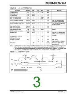
TABLE 1-2:
DC CHARACTERISTICS
VCC = +5V (±10%)
Commercial (C): Tamb = 0°C to +70°C
Industrial (I): Tamb = -40°C to +85°C
Automotive (E): Tamb = -40°C to +125°C
Parameter
Symbol
Min.
Max.
Units
Conditions
VCC detector threshold
VTH
2.8
4.5
V
SCL and SDA pins:
High level input voltage
Low level input voltage
Low level output voltage
VIH
VIL
VOL
VCC x 0.7 VCC + 1
V
V
V
-0.3
VCC x 0.3
0.4
IOL = 3.2 mA (SDA only)
A1 & A2 pins:
High level input voltage
Low level input voltage
VIH
VIL
VCC - 0.5 VCC + 0.5
V
V
-0.3
0.5
Input leakage current
Output leakage current
ILI
—
10
µA
µA
pF
VIN = 0V to VCC
ILO
—
10
VOUT = 0V to VCC
Pin capacitance
CIN,
—
7.0
VIN/VOUT = 0V (Note)
(all inputs/outputs)
COUT
Tamb = +25˚C, f = 1 MHz
Operating current
ICC Write
—
—
—
—
3.5
4.25
750
100
mA
mA
µA
FCLK = 100 kHz, program cycle time = 1 ms,
Vcc = 5V, Tamb = 0˚C to +70˚C
ICC Write
FCLK = 100 kHz, program cycle time = 1 ms,
Vcc = 5V, Tamb = (I) and (E)
ICC
Read
VCC = 5V, Tamb= (C), (I) and (E)
Standby current
ICCS
µA
SDA=SCL=VCC=5V (no PROGRAM active)
Note: This parameter is periodically sampled and not 100% tested
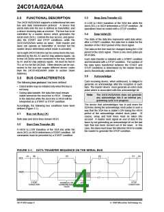
FIGURE 1-1: BUS TIMING START/STOP
VHYS
SCL
SDA
THD:STA
TSU:STA
TSU:STO
START
STOP
DS11183D-page 2
1996 Microchip Technology Inc.

 MICROCHIP [ MICROCHIP ]