PIC12CE67X
12.5
Timing Parameter Symbology
The timing parameter symbols have been created following one of the following formats:
2
1. TppS2ppS
2. TppS
3. TCC:ST
4. Ts
(I C specifications only)
2
(I C specifications only)
T
F
Frequency
T
Time
Lowercase letters (pp) and their meanings:
pp
cc
CCP1
CLKOUT
CS
osc
rd
OSC1
RD
ck
cs
di
rw
sc
ss
t0
RD or WR
SCK
SDI
do
dt
SDO
SS
Data in
I/O port
MCLR
T0CKI
T1CKI
WR
io
t1
mc
wr
Uppercase letters and their meanings:
S
F
H
I
Fall
P
R
V
Z
Period
High
Rise
Invalid (Hi-impedance)
Low
Valid
L
Hi-impedance
2
I C only
AA
output access
Bus free
High
Low
High
Low
BUF
2
TCC:ST (I C specifications only)
CC
HD
ST
DAT
STA
Hold
SU
Setup
DATA input hold
START condition
STO
STOP condition
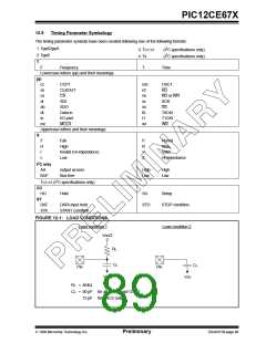
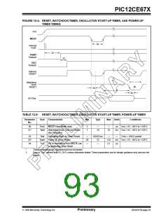
FIGURE 12-1: LOAD CONDITIONS
Load condition 1
Load condition 2
VDD/2
RL
CL
CL
Pin
Pin
VSS
VSS
RL = 464Ω
CL = 50 pF for all pins except OSC2
15 pF for OSC2 output
1998 Microchip Technology Inc.
Preliminary
DS40181B-page 89

 MICROCHIP [ MICROCHIP ]