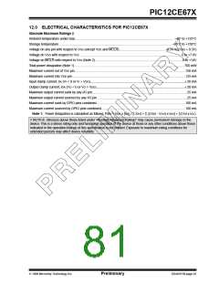
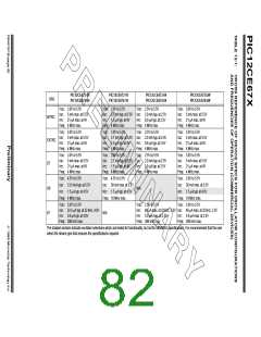
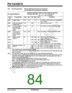
PIC12CE67X
(4)
12.3
DC Characteristics:
PIC12CE673-04 (Commercial, Industrial, Extended )
(4)
PIC12CE673-10 (Commercial, Industrial, Extended )
(4)
PIC12CE674-04 (Commercial, Industrial, Extended )
(4)
PIC12CE674-10 (Commercial, Industrial, Extended )
Standard Operating Conditions (unless otherwise specified)
Operating temperature
0˚C ≤ TA ≤ +70˚C (commercial)
–40˚C ≤ TA ≤ +85˚C (industrial)
–40°C ≤ TA ≤ +125˚C (extended)
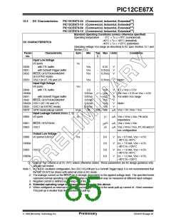
DC CHARACTERISTICS
Operating voltage VDD range as described in DC spec Section 12.1 and
Section 12.2.
Param
No.
Characteristic
Sym
Min
Typ Max Units
†
Conditions
Input Low Voltage
I/O ports
VIL
D030
D031
D032
with TTL buffer
VSS
VSS
VSS
-
-
-
0.5V
0.2VDD
0.2VDD
V
V
V
with Schmitt Trigger buffer
MCLR, GP2/T0CKI/AN2/INT
(in EXTRC mode)
OSC1 (in XT, HS and LP)
Input High Voltage
I/O ports
D033
VSS
-
0.3VDD
V
Note1
VIH
-
-
-
-
-
-
-
D040
D040A
D041
D042
with TTL buffer
2.0
VDD
VDD
VDD
VDD
VDD
VDD
V
V
V
V
V
V
4.5 ≤ VDD ≤ 5.5V
For VDD > 5.5V or VDD < 4.5V
For entire VDD range
0.8VDD
0.8VDD
0.8VDD
0.7VDD
0.9VDD
50
with Schmitt Trigger buffer
MCLR, GP2/T0CKI/AN2/INT
D042A OSC1 (XT, HS and LP)
D043
D070
Note1
OSC1 (in EXTRC mode)
GPIO weak pull-up current
Input Leakage Current (Notes 2, 3)
I/O ports
IPUR
IIL
250 400
µA VDD = 5V, VPIN = VSS
D060
-
-
+1
µA Vss ≤ VPIN ≤ VDD, Pin at hi-
impedance
(5)
D061
D063
MCLR, GP2/T0CKI
OSC1
-
-
-
-
µA Vss ≤ VPIN ≤ VDD
+5
+5
µA Vss ≤ VPIN ≤ VDD, XT, HS and LP
osc configuration
Output Low Voltage
D080
D080A
D083
D083A
†
I/O ports/CLKOUT
VOL
-
-
-
-
-
-
-
-
0.6
0.6
0.6
0.6
V
V
V
V
IOL = 8.5 mA, VDD = 4.5V,
–40°C to +85°C
IOL = 7.0 mA, VDD = 4.5V,
–40°C to +125°C
IOL = 1.6 mA, VDD = 4.5V,
–40°C to +85°C
IOL = 1.2 mA, VDD = 4.5V,
–40°C to +125°C
OSC2
Data in “Typ” column is at 5V, 25°C unless otherwise stated. These parameters are for design guidance only
and are not tested.
Note 1: In EXTRC oscillator configuration, the OSC1/CLKIN pin is a Schmitt Trigger input. It is not recommended that
the PIC12C67X be driven with external clock in RC mode.
2: The leakage current on the MCLR pin is strongly dependent on the applied voltage level. The specified levels
represent normal operating conditions. Higher leakage current may be measured at different input voltages.
3: Negative current is defined as coming out of the pin.
4: Extended operating range is Advance Information for this device.
5: When configured as external reset, the input leakage current is the weak pulll-up current of -10mA minimum.
This pull-up is weaker than the standard I/O pull-up.
1998 Microchip Technology Inc.
Preliminary
DS40181B-page 85

 MICROCHIP [ MICROCHIP ]