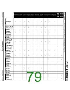
PIC12CE67X
(5)
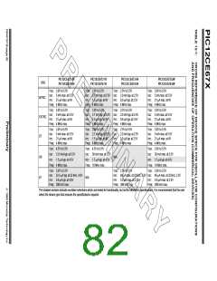
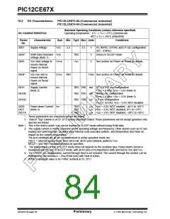
12.1
DC Characteristics:
PIC12CE673-04 (Commercial, Industrial, Extended )
(5)
(5)
(5)
PIC12CE673-10 (Commercial, Industrial, Extended
PIC12CE674-04 (Commercial, Industrial, Extended
PIC12CE674-10 (Commercial, Industrial, Extended
)
)
)
Standard Operating Conditions (unless otherwise specified)
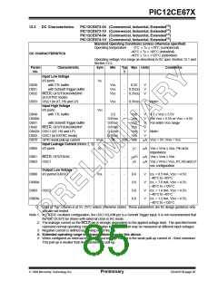
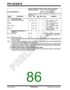
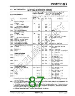
DC CHARACTERISTICS
Operating temperature
0˚C ≤ TA ≤ +70˚C (commercial)
–40˚C ≤ TA ≤ +85˚C (industrial)
–40°C ≤ TA ≤ +125˚C (extended)
Parm
No.
Characteristic
Sym Min Typ† Max Units
Conditions
D001
Supply Voltage
VDD 3.0
4.5
-
-
5.5
V
XT, INTRC, EXTRC and LP osc configura-
tion
HS osc configuration
D001A
D002
5.5
-
V
V
RAM Data Retention
Voltage (Note 1)
VDR
-
1.5
-
Device in SLEEP mode
D003
VDD start voltage to
ensure internal Power-on
Reset signal
VPO VSS
R
VSS
V
See section on Power-on Reset for details
D004
D010
VDD rise rate to ensure inter- SVD 0.05
-
-
V/ms See section on Power-on Reset for details
nal Power-on Reset signal
D
Supply Current (Note 2)
No read/write to EEPROM
peripheral
IDD
-
2.7
3.3
mA XT, EXTRC osc configuration
(PIC12CE67X-04)
FOSC = 4 MHz, VDD = 5.5V (Note 4)
mA INTRC osc configuration
FOSC = 4 MHz, VDD = 5.5V (Note 6)
mA HS osc configuration (PIC12CE67X-10)
FOSC = 10 MHz, VDD = 5.5V
D010A
D013
2.7
3.3
-
TBD 15
D028
∆IEE
0.1
0.2
VDD = 5.5V
SCL = 400 kHz
D020
D021
D021A
D021B
Power-down Current (Note 3) IPD
-
-
-
-
5.5
1.5
1.5
32
16
14
µA VDD = 4.0V, WDT enabled, –40°C to +85°C
µA VDD = 4.0V, WDT disabled, 0°C to +70°C
µA VDD = 4.0V, WDT disabled, –40°C to
1.5 TBD µA +85°C
VDD = 4.0V, WDT disabled, –40°C to
+125°C
*
These parameters are characterized but not tested.
†
Data in "Typ" column is at 5V, 25˚C unless otherwise stated. These parameters are for design guidance only
and are not tested.
Note 1: This is the limit to which VDD can be lowered in SLEEP mode without losing RAM data.
2: The supply current is mainly a function of the operating voltage and frequency. Other factors such as I/O pin
loading and switching rate, oscillator type, internal code execution pattern, and temperature also have an
impact on the current consumption.
The test conditions for all IDD measurements in active operation mode are:
OSC1 = external square wave, from rail to rail; all I/O pins tristated, pulled to VDD
MCLR = VDD; WDT enabled/disabled as specified.
3: The power-down current in SLEEP mode does not depend on the oscillator type. Power-down current is
measured with the part in SLEEP mode, with all I/O pins in hi-impedance state and tied to VDD and VSS.
4: For EXTRC osc configuration, current through Rext is not included. The current through the resistor can be
estimated by the formula Ir = VDD/2Rext (mA) with Rext in kOhm.
5: Extended operating range is Advance Information for this device.
6: INTRC calibration value is for 4 MHz nominal at 5V, 35°C.
1998 Microchip Technology Inc.
Preliminary
DS40181B-page 83

 MICROCHIP [ MICROCHIP ]