PIC12CE67X
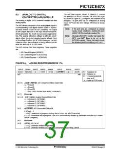
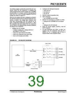
The ADCON0 register, shown in Figure 8-1, controls
the operation of the A/D module. The ADCON1 regis-
ter, shown in Figure 8-2, configures the functions of the
port pins. The port pins can be configured as analog
inputs (GP1 can also be a voltage reference) or as dig-
ital I/O.
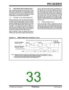
8.0
ANALOG-TO-DIGITAL
CONVERTER (A/D) MODULE
The analog-to-digital (A/D) converter module has four
analog inputs.
The A/D allows conversion of an analog input signal to
a corresponding 8-bit digital number (refer to Applica-
tion Note AN546 for use of A/D Converter). The output
of the sample and hold is the input into the converter,
which generates the result via successive approxima-
tion. The analog reference voltage is software select-
able to either the device’s positive supply voltage (VDD)
or the voltage level on the GP1/AN1/VREF pin.The A/D
converter has a unique feature of being able to operate
while the device is in SLEEP mode.
Note: If the port pins are configured as analog
inputs (reset condition), reading the port
(MOVF GP,W) results in reading '0's.
Note: Changing ADCON1 register can cause the
GPIF and INTF flags to be set in the
INTCON register. These interrupts should
be disabled prior to modifying ADCON1.
The A/D module has three registers. These registers
are:
• A/D Result Register (ADRES)
• A/D Control Register 0 (ADCON0)
• A/D Control Register 1 (ADCON1)
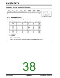
FIGURE 8-1: ADCON0 REGISTER (ADDRESS 1Fh)
R/W-0 R/W-0 R/W-0
R/W-0
CHS1
R/W-0
R/W-0
R/W-0
r
R/W-0
ADON
ADCS1 ADCS0
bit7
r
CHS0 GO/DONE
R =Readable bit
W = Writable bit
U =Unimplemented bit,
read as ‘0’
bit0
- n = Value at POR reset
bit 7-6: ADCS1:ADCS0: A/D Conversion Clock Select bits
00= FOSC/2
01= FOSC/8
10= FOSC/32
11= FRC (clock derived from an RC oscillation)
bit 5:
Reserved
bit 4-3: CHS1:CHS0: Analog Channel Select bits
00= channel 0, (GP0/AN0)
01= channel 1, (GP1/AN1)
10= channel 2, (GP2/AN2)
11= channel 3, (GP4/AN3)
bit 2:
GO/DONE: A/D Conversion Status bit
If ADON = 1
1 = A/D conversion in progress (setting this bit starts the A/D conversion)
0 = A/D conversion not in progress (This bit is automatically cleared by hardware when the A/D conver-
sion is complete)
bit 1:
bit 0:
Reserved
ADON: A/D On bit
1 = A/D converter module is operating
0 = A/D converter module is shutoff and consumes no operating current
1998 Microchip Technology Inc.
Preliminary
DS40181B-page 37

 MICROCHIP [ MICROCHIP ]