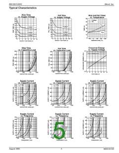
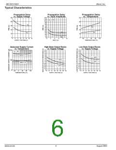
MIC4421/4422
Micrel, Inc.
Electrical Characteristics: (Over operating temperature range with 4.5V ≤ VS ≤ 18V unless otherwise specified.)
Symbol
INPUT
VIH
Parameter
Conditions
Min
Typ
Max
Units
Logic 1 Input Voltage
Logic 0 Input Voltage
Input Voltage Range
Input Current
2.4
1.4
1.0
V
V
VIL
0.8
VS+0.3
10
VIN
–5
V
IIN
0V ≤ VIN ≤ VS
–10
µA
OUTPUT
VOH
High Output Voltage
Low Output Voltage
Figure 1
VS–.025
V
V
Ω
VOL
Figure 1
0.025
3.6
RO
Output Resistance,
Output High
IOUT = 10mA, VS = 18V
0.8
1.3
RO
Output Resistance,
Output Low
IOUT = 10mA, VS = 18V
2.7
Ω
SWITCHING TIME (Note 3)
tR
Rise Time
Fall Time
Figure 1, CL = 10,000pF
Figure 1, CL = 10,000pF
Figure 1
23
30
20
40
120
120
80
ns
ns
ns
ns
tF
tD1
tD2
Delay Time
Delay Time
Figure 1
80
POWER SUPPLY
IS
Power Supply Current
VIN = 3V
0.6
0.1
3
0.2
mA
V
VIN = 0V
VS
Operating Input Voltage
4.5
18
Note 1:
Note 2:
Functional operation above the absolute maximum stress ratings is not implied.
Static-sensitive device. Store only in conductive containers. Handling personnel and equipment should be grounded to
prevent damage from static discharge.
Note 3:
Switching times guaranteed by design.
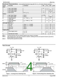
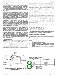
Test Circuits
VS = 18V
VS = 18V
0.1µF
4.7µF
0.1µF
4.7µF
0.1µF
0.1µF
IN
OUT
15000pF
IN
OUT
15000pF
MIC4421
MIC4422
5V
90%
5V
90%
2.5V
tPW≥ 0.5µs
2.5V
tPW≥ 0.5µs
INPUT
INPUT
10%
0V
10%
0V
tPW
tPW
tD1
tF
tD2
tR
tD1
tF
tR
tD2
VS
VS
90%
90%
OUTPUT
OUTPUT
10%
0V
10%
0V
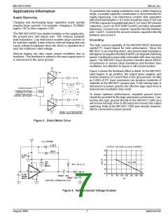
Figure 2. Noninverting Driver Switching Time
August 2005
Figure 1. Inverting Driver Switching Time
M9999-081005
4

 MIC [ MIC GROUP RECTIFIERS ]