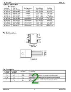
MIC4421/4422
Micrel, Inc.
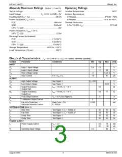
Absolute Maximum Ratings (Notes 1, 2 and 3)
Supply Voltage ..............................................................20V
Input Voltage ...................................VS + 0.3V to GND – 5V
Input Current (VIN > VS).............................................. 50 mA
Power Dissipation, TA ≤ 25°C
Operating Ratings
Junction Temperature................................................ 150°C
Ambient Temperature
C Version.................................................... 0°C to +70°C
B Version ................................................ –40°C to +85°C
Thermal Resistance
PDIP ....................................................................960mW
SOIC..................................................................1040mW
5-Pin TO-220 ..............................................................2W
Power Dissipation, TCASE ≤ 25°C
5-Pin TO-220 (θJC) ...............................................10°C/W
5-Pin TO-220 .........................................................12.5W
Derating Factors (to Ambient)
PDIP ................................................................7.7mW/°C
SOIC................................................................8.3mW/°C
5-Pin TO-220 ....................................................17mW/°C
Storage Temperature................................ –65°C to +150°C
Lead Temperature (10 sec) ....................................... 300°C
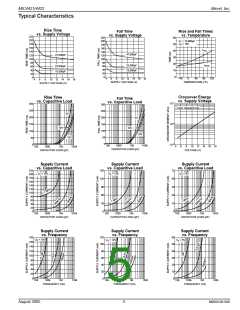
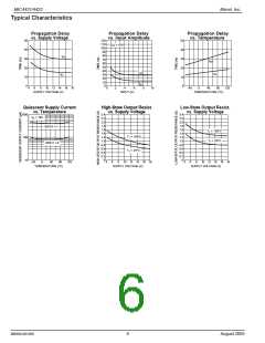
Electrical Characteristics: (TA = 25°C with 4.5 V ≤ VS ≤ 18 V unless otherwise specified.)
Symbol
INPUT
VIH
Parameter
Conditions
Min
Typ
Max
Units
Logic 1 Input Voltage
Logic 0 Input Voltage
Input Voltage Range
Input Current
2.4
1.3
1.1
V
V
VIL
0.8
VS+0.3
10
VIN
–5
V
IIN
0 V ≤ VIN ≤ VS
–10
µA
OUTPUT
VOH
High Output Voltage
Low Output Voltage
See Figure 1
VS–.025
V
V
Ω
VOL
See Figure 1
0.025
1.7
RO
Output Resistance,
Output High
IOUT = 10 mA, VS = 18 V
0.6
0.8
9
RO
Output Resistance,
Output Low
IOUT = 10 mA, VS = 18 V
VS = 18 V (See Figure 6)
Ω
IPK
IDC
IR
Peak Output Current
A
A
Continuous Output Current
2
Latch-Up Protection
Withstand Reverse Current
Duty Cycle ≤ 2%
t ≤ 300 µs
>1500
mA
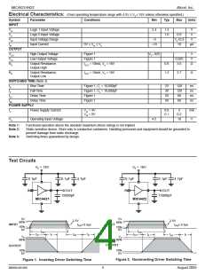
SWITCHING TIME (Note 3)
tR
Rise Time
Fall Time
Test Figure 1, CL = 10,000 pF
Test Figure 1, CL = 10,000 pF
Test Figure 1
20
24
15
35
75
75
60
60
ns
ns
ns
ns
tF
tD1
tD2
Delay Time
Delay Time
Test Figure 1
POWER SUPPLY
IS
Power Supply Current
VIN = 3 V
0.4
80
1.5
150
mA
µA
VIN = 0 V
VS
Operating Input Voltage
4.5
18
V
August 2005
3
M9999-081005

 MIC [ MIC GROUP RECTIFIERS ]