MIC4421/4422
Micrel, Inc.
Input Stage
dissipation limit can easily be exceeded. Therefore, some
attention should be given to power dissipation when driving
low impedance loads and/or operating at high frequency.
The input voltage level of the MIC4421 changes the quies-
cent supply current. The N channel MOSFET input stage
transistor drives a 320µA current source load. With a logic
“1” input, the maximum quiescent supply current is 400µA.
Logic “0” input level signals reduce quiescent current to
80µA typical.
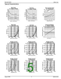
The supply current vs. frequency and supply current vs
capacitive load characteristic curves aid in determining
power dissipation calculations. Table 1 lists the maximum
safe operating frequency for several power supply volt-
ages when driving a 10,000pF load. More accurate power
dissipation figures can be obtained by summing the three
dissipation sources.
The MIC4421/4422 input is designed to provide 300mV of
hysteresis. This provides clean transitions, reduces noise
sensitivity, and minimizes output stage current spiking
when changing states. Input voltage threshold level is ap-
proximately 1.5V, making the device TTL compatible over
the full temperature and operating supply voltage ranges.
Input current is less than ±10µA.
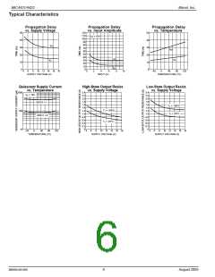
Given the power dissipation in the device, and the thermal
resistance of the package, junction operating temperature
for any ambient is easy to calculate. For example, the
thermal resistance of the 8-pin plastic DIP package, from
the data sheet, is 130°C/W. In a 25°C ambient, then, using
a maximum junction temperature of 150°C, this package
will dissipate 960mW.
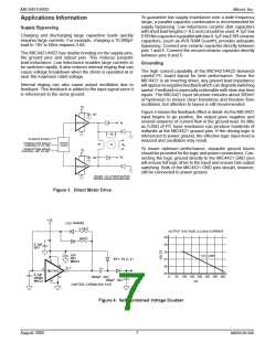
The MIC4421 can be directly driven by the TL494,
SG1526/1527, SG1524, TSC170, MIC38C42, and similar
switchmodepowersupplyintegratedcircuits. Byoffloading
the power-driving duties to the MIC4421/4422, the power
supply controller can operate at lower dissipation. This can
improve performance and reliability.
Accurate power dissipation numbers can be obtained by
summing the three sources of power dissipation in the
device:
The input can be greater than the VS supply, however, cur-
rent will flow into the input lead. The input currents can be
as high as 30mAp-p (6.4mA ) with the input. No damage
will occur to MIC4421/4422RhMoSwever, and it will not latch.
• Load Power Dissipation (PL)
• Quiescent power dissipation (P )
• Transition power dissipation (PTQ)
Calculation of load power dissipation differs depending on
whether the load is capacitive, resistive or inductive.
The input appears as a 7pF capacitance and does not
change even if the input is driven from an AC source.
While the device will operate and no damage will occur up
to 25V below the negative rail, input current will increase
up to 1mA/V due to the clamping action of the input, ESD
diode, and 1kΩ resistor.
Resistive Load Power Dissipation
Dissipation caused by a resistive load can be calculated
as:
PL = I2 RO D
where:
Power Dissipation
CMOS circuits usually permit the user to ignore power
dissipation. Logic families such as 4000 and 74C have out-
puts which can only supply a few milliamperes of current,
and even shorting outputs to ground will not force enough
current to destroy the device. The MIC4421/4422 on the
other hand, can source or sink several amperes and drive
largecapacitiveloadsathighfrequency.Thepackagepower
I = the current drawn by the load
RO = the output resistance of the driver when the output
is high, at the power supply voltage used. (See data
sheet)
D = fraction of time the load is conducting (duty cycle)
+18
WIMA
MKS-2
1 µF
5.0V
18 V
1
TEK CURRENT
PROBE 6302
8
5
6, 7
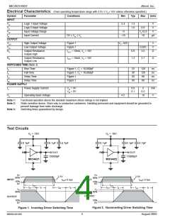
Table 1: MIC4421 Maximum
Operating Frequency
MIC4421
4
0 V
0 V
0.1µF
0.1µF
VS
Max Frequency
220kHz
2,500 pF
POLYCARBONATE
18V
15V
10V
5V
LOGIC
GROUND
6 AMPS
PC TRACE RESISTANCE = 0.05Ω
300kHz
300 mV
640kHz
POWE
R
GROUND
2MHz
Conditions:
1. θJA = 150°C/W
2. TA = 25°C
3. CL = 10,000pF
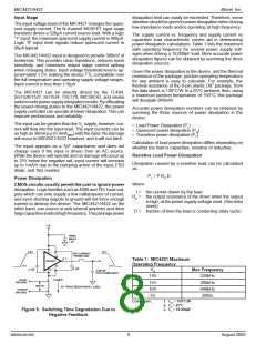
Figure 5. Switching Time Degradation Due to
Negative Feedback
M9999-081005
8
August 2005

 MIC [ MIC GROUP RECTIFIERS ]