MX29LV640BT/BB
ware reset immediately terminates the programming
operation.The Byte/Word Program command sequence
should be reinitiated once the device has reset to read-
ing array data, to ensure data integrity.
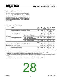
tion Status" for information on these status bits. When
the Automatic Erase algorithm is complete, the device
returns to reading array data and addresses are no longer
latched.
Programming is allowed in any sequence and across
sector boundaries. A bit cannot be programmed from a
"0" back to a "1". Attempting to do so may halt the op-
eration and set Q5 to "1" ,” or cause the Data# Polling
algorithm to indicate the operation was successful. How-
ever, a succeeding read will show that the data is still
"0". Only erase operations can convert a "0" to a "1".
Figure 5 illustrates the algorithm for the erase operation.
See the Erase/Program Operations tables in "AC Char-
acteristics" for parameters, and to Figure 4 for timing
diagrams.
SECTOR ERASE COMMANDS
The Automatic Sector Erase does not require the device
to be entirely pre-programmed prior to executing the Au-
tomatic Set-up Sector Erase command and Automatic
Sector Erase command. Upon executing the Automatic
Sector Erase command, the device will automatically pro-
gram and verify the sector(s) memory for an all-zero data
pattern. The system is not required to provide any con-
trol or timing during these operations.
SETUP AUTOMATIC CHIP/SECTOR ERASE
Chip erase is a six-bus cycle operation. There are two
"unlock" write cycles. These are followed by writing the
"set-up" command 80H. Two more "unlock" write cycles
are then followed by the chip erase command 10H, or
the sector erase command 30H.
The MX29LV640BT/BB contains a Silicon-ID-Read op-
eration to supplement traditional PROM programming
methodology. The operation is initiated by writing the
read silicon ID command sequence into the command
register. Following the command write, a read cycle with
A1=VIL,A0=VIL retrieves the manufacturer code of C2H.
A read cycle with A1=VIL, A0=VIH returns the device
code of 22C9H/22CBH for MX29LV640BT/BB.
When the sector(s) is automatically verified to contain an
all-zero pattern, a self-timed sector erase and verify be-
gin. The erase and verify operations are complete when
the data on Q7 is "1" and the data on Q6 stops toggling
for two consecutive read cycles, at which time the de-
vice returns to the Read mode. The system is not re-
quired to provide any control or timing during these opera-
tions.
When using the Automatic Sector Erase algorithm, note
that the erase automatically terminates when adequate
erase margin has been achieved for the memory array
(no erase verification command is required). Sector erase
is a six-bus cycle operation. There are two "unlock" write
cycles. These are followed by writing the set-up com-
mand 80H. Two more "unlock" write cycles are then fol-
lowed by the sector erase command 30H. The sector
address is latched on the falling edge of WE# or CE#,
whichever happens later , while the command (data) is
latched on the rising edge of WE# or CE#, whichever
happens first. Sector addresses selected are loaded
into internal register on the sixth falling edge of WE# or
CE#, whichever happens later. Each successive sector
load cycle started by the falling edge of WE# or CE#,
whichever happens later must begin within 50us from
the rising edge of the preceding WE# or CE#, whichever
happens first. Otherwise, the loading period ends and
internal auto sector erase cycle starts. (Monitor Q3 to
determine if the sector erase timer window is still open,
see section Q3, Sector EraseTimer.) Any command other
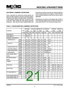
AUTOMATIC CHIP/SECTOR ERASE COM-
MAND
The device does not require the system to preprogram
prior to erase.The Automatic Erase algorithm automati-
cally pre-program and verifies the entire memory for an
all zero data pattern prior to electrical erase.The system
is not required to provide any controls or timings during
these operations. Table 3 shows the address and data
requirements for the chip erase command sequence.
Any commands written to the chip during the Automatic
Erase algorithm are ignored.Note that a hardware reset
during the chip erase operation immediately terminates
the operation.The Chip Erase command sequence should
be reinitiated once the device has returned to reading
array data, to ensure data integrity.
The system can determine the status of the erase opera-
tion by using Q7, Q6, Q2, or RY/BY#.See "Write Opera-
P/N:PM1076
REV. 1.2, SEP. 07, 2005
24

 Macronix [ MACRONIX INTERNATIONAL ]