MX29LV640BT/BB
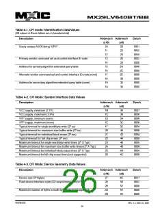
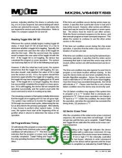
Table 4-1. CFI mode: Identification Data Values
(All values in these tables are in hexadecimal)
Description
Addressh Addressh
Datah
(x16)
10
(x8)
20
22
24
26
28
2A
2C
2E
30
32
34
Query-unique ASCII string "QRY"
0051
0052
0059
0002
0000
0040
0000
0000
0000
0000
0000
11
12
Primary vendor command set and control interface ID code
Address for primary algorithm extended query table
13
14
15
16
Alternate vendor command set and control interface ID code (none)
Address for secondary algorithm extended query table (none)
17
18
19
1A
Table 4-2. CFI Mode: System Interface Data Values
Description
Addressh Addressh
Datah
(x16)
1B
1C
1D
1E
1F
20
(x8)
36
VCC supply, minimum (2.7V)
0027
0036
0000
0000
0004
0000
000A
0000
0005
0000
0004
0000
VCC supply, maximum (3.6V)
38
VPP supply, minimum (none)
3A
3C
3E
40
VPP supply, maximum (none)
Typical timeout for single word/byte write (2N us)
Typical timeout for maximum size buffer write (2N us)
Typical timeout for individual block erase (2N ms)
Typical timeout for full chip erase (2N ms)
Maximum timeout for single word/byte write times (2N X Typ)
Maximum timeout for maximum size buffer write times (2N X Typ)
Maximum timeout for individual block erase times (2N X Typ)
Maximum timeout for full chip erase times (not supported)
21
42
22
44
23
46
24
48
25
4A
4C
26
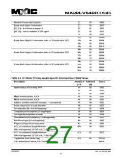
Table 4-3. CFI Mode: Device Geometry Data Values
Description
Addressh Addressh
Datah
(x16)
27
(x8)
4E
50
Device size (2n bytes)
0017
0002
0000
0000
0000
Flash device interface code (02=asynchronous x8/x16)
28
29
52
Maximum number of bytes in multi-byte write (not supported)
2A
2B
54
56
P/N:PM1076
REV. 1.2, SEP. 07, 2005
26

 Macronix [ MACRONIX INTERNATIONAL ]