MX29LV640BT/BB
Erase Resume (30H) commands are valid only while the
Sector Erase operation is in progress. Either of the two
reset command sequences will reset the device (when
applicable).
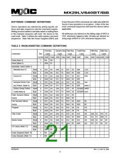
SOFTWARE COMMAND DEFINITIONS
Device operations are selected by writing specific ad-
dress and data sequences into the command register.
Writing incorrect address and data values or writing them
in the improper sequence will reset the device to the
read mode. Table 3 defines the valid register command
sequences. Note that the Erase Suspend (B0H) and
All addresses are latched on the falling edge of WE# or
CE#, whichever happens later. All data are latched on
rising edge of WE# or CE#, whichever happens first.
TABLE 3. MX29LV640BT/BB COMMAND DEFINITIONS
First Bus
Cycle
Second Bus Third Bus
Cycle Cycle
Fourth Bus
Cycle
Fifth Bus Sixth Bus
Cycle Cycle
Command
Bus
Cycles Addr Data Addr Data Addr Data Addr
Data Addr Data Addr Data
Read (Note 5)
1
1
RA
RD
Reset (Note 6)
XXX F0
Automatic Select (Note 7)
Manufacturer ID
Word
Byte
4
4
4
4
4
4
4
4
3
3
4
4
4
4
6
6
6
6
1
1
1
1
555 AA
AAA AA
555 AA
AAA AA
555 AA
AAA AA
555 AA
AAA AA
555 AA
AAA AA
555 AA
AAA AA
555 AA
AAA AA
555 AA
AAA AA
555 AA
AAA AA
2AA 55
555 55
2AA 55
555 55
2AA 55
555 55
2AA 55
555 55
2AA 55
555 55
2AA 55
555 55
2AA 55
555 55
2AA 55
555 55
2AA 55
555 55
555 90
AAA 90
555 90
AAA 90
555 90
AAA 90
555 90
AAA 90
555 88
AAA 88
555 90
AAA 90
555 A0
AAA A0
555 80
AAA 80
555 80
AAA 80
X00
X00
X01
X02
X03
X06
C2H
C2H
DDI
Device ID
Word
Byte
Secured Sector Fact- Word
see
ory Protect (Note 9)
Sector Group Protect
Verify (Note 8)
Enter Secured Silicon
Sector
Byte
Word
Byte
Word
Byte
Word
Byte
Word
Byte
Word
Byte
Word
Byte
Word
Byte
note 9
(SA)X02 xx00/
(SA)X04 xx01
Exit Secured Silicon
Sector
XXX
XXX
PA
00
00
Program
PD
PD
AA
AA
AA
AA
PA
Chip Erase
555
AAA
555
AAA
2AA 55 555 10
555 55 AAA 10
2AA 55 SA 30
555 55 SA 30
Sector Erase
CFI Query (Note 12)
55
98
98
B0
30
AA
BA
BA
Erase Suspend (Note 10)
Erase Resume (Note 11)
P/N:PM1076
REV. 1.2, SEP. 07, 2005
21

 Macronix [ MACRONIX INTERNATIONAL ]