MX25L8005
• WP# pin
- Hardware write protection
• HOLD# pin
- pause the chip without diselecting the chip
• PACKAGE
- 8-pin SOP (150mil)
- 8-pin SOP (200mil)
- 8-pin PDIP (300mil)
- 8-land SON/WSON (6x5mm), 8-land SON is not recommended for new design
- 8-land USON (4x4mm)
- All Pb-free devices are RoHS Compliant
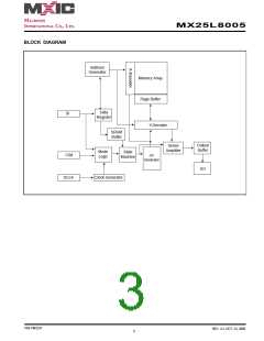
GENERAL DESCRIPTION
The MX25L8005 is a CMOS 8,388,608 bit serial Flash memory, which is configured as 1,048,576 x 8 internally. The
MX25L8005featureaserialperipheralinterfaceandsoftwareprotocolallowingoperationonasimple3-wirebus.Thethree
bus signals are a clock input (SCLK), a serial data input (SI), and a serial data output (SO). SPI access to the device is
enabled by CS# input.
The MX25L8005 provide sequential read operation on whole chip.
After program/erase command is issued, auto program/ erase algorithms which program/ erase and verify the specified
pageorbyte/sector/blocklocationswillbeexecuted.Programcommandisexecutedonpage(256bytes)basis,anderase
command is executes on chip or sector(4K-bytes) or block(64K-bytes).
To provide user with ease of interface, a status register is included to indicate the status of the chip. The status read
command can be issued to detect completion status of a program or erase operation via WIP bit.
When the device is not in operation and CS# is high, it is put in standby mode and draws less than 10uA DC current.
TheMX25L8005utilizeMXIC'sproprietarymemorycell,whichreliablystoresmemorycontentsevenafter100,000program
and erase cycles.
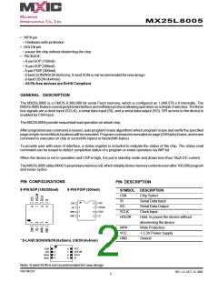
PIN CONFIGURATIONS
8-PINSOP(150/200mil)
PIN DESCRIPTION
8-PIN PDIP (300mil)
SYMBOL DESCRIPTION
CS#
SI
Chip Select
Serial Data Input
Serial Data Output
Clock Input
1
2
3
4
VCC
HOLD#
SCLK
SI
CS#
SO
8
7
6
5
SO
WP#
GND
SCLK
HOLD#
Hold, to pause the device without
deselecting the device
WriteProtection
+ 3.3V Power Supply
Ground
WP#
VCC
GND
*8-LANDSON/WSON(6x5mm),USON(4x4mm)
1
2
3
4
VCC
HOLD#
SCLK
SI
CS#
SO
8
7
6
5
WP#
GND
Note: 8-land SON is not recommended for new design
P/N:PM1237
REV. 2.2, OCT. 23, 2008
2

 Macronix [ MACRONIX INTERNATIONAL ]