MX25L12835F
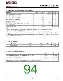
14. ERASE AND PROGRAMMING PERFORMANCE
Parameter
Min.
Typ. (1)
Max. (2)
40
Unit
ms
ms
s
Write Status Register Cycle Time
Sector Erase Cycle Time (4KB)
Block Erase Cycle Time (32KB)
Block Erase Cycle Time (64KB)
Chip Erase Cycle Time
43
0.19
0.34
72
200
1
2
s
160
30
s
Byte Program Time (via page program command)
Page Program Time
12
us
0.6
3
ms
cycles
Erase/Program Cycle
100,000
Note:
1. Typical program and erase time assumes the following conditions: 25 C, 3.3V, and all zero pattern.
°
2. Under worst conditions of 85 C and 2.7V.
°
3. System-level overhead is the time required to execute the first-bus-cycle sequence for the programming com-
mand.
4. The maximum chip programming time is evaluated under the worst conditions of 0°C, VCC=3.3V, and 100K cy-
cle with 90% confidence level.
15. DATA RETENTION
Parameter
Condition
Min.
Max.
Unit
Data retention
55˚C
20
years
16. LATCH-UP CHARACTERISTICS
Min.
Max.
Input Voltage with respect to GND on all power pins, SI, CS#
Input Voltage with respect to GND on SO
Current
-1.0V
-1.0V
2 VCCmax
VCC + 1.0V
+100mA
-100mA
Includes all pins except VCC. Test conditions: VCC = 3.0V, one pin at a time.
P/N: PM1795
REV. 1.0, OCT. 23, 2012
94

 Macronix [ MACRONIX INTERNATIONAL ]