Smallest TEC Power Drivers for
Optical Modules
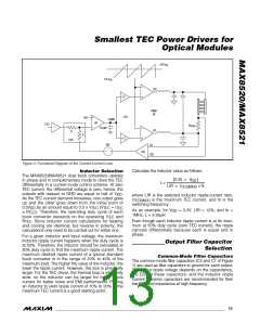
6) To ensure high DC loop gain and minimum loop
error, keep the board layout adjacent to the negative
input pin of the integrator (U2 in Figure1) clean and
free of moisture. Any contamination or leakage
current into this node can act to lower the DC gain of
the integrator, which can degrade the accuracy of
the thermal loop. If space is available, it can also be
helpful to surround the negative input node of the
integrator with a grounded guard ring.
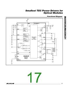
Refer to the MAX8520/MAX8521 evaluation kit for a PC
board layout example.
Chip Information
TRANSISTOR COUNT: 3007
PROCESS: BiCMOS
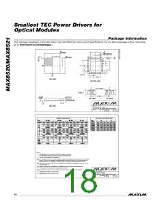
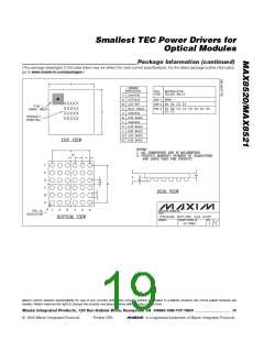
Pin Configurations
TOP VIEW
MAX8521
F6
PV
F5
PV
F4
CS
F3
F2
F1
PV
2
DD
2
DD
OS1 PV
1
1
DD
DD
LX1
PGND1
SHDN
COMP
ITEC
1
2
3
4
5
15 LX2
E6
LX2
E5
LX2
E4
N.C.
E3
N.C.
E2
LX1
E1
LX1
14 PGND2
13 FREQ
D6
D5
D4
D3
D2
D1
MAX8520/
MAX8521
PGND2 PGND2 PGND2 PGND1 PGND1 PGND1
12
11
V
DD
C6
OS2
C5
C4
C3
C2
C1
SHDN
GND
FREQ GND2 GND2 COMP
B6
B5
B4
B3
B2
B1
VDD GND2 N.C.
N.C. GND2 ITEC
A6
A5
A4
A3 A2 A1
GND
CTLI
REF MAXV MAXIP MAXIN
THIN QFN
UCSP
16 ______________________________________________________________________________________

 MAXIM [ MAXIM INTEGRATED PRODUCTS ]