Smallest TEC Power Drivers for
Optical Modules
Take care not to exceed the positive or negative cur-
Applications Information
rent limit on the TEC. Refer to the manufacturer’s data
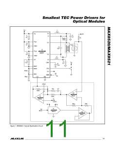
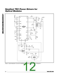
The MAX8520/MAX8521 typically drive a TEC inside a
thermal-control loop. TEC drive polarity and power are
regulated based on temperature information read from a
thermistor or other temperature-measuring device to
maintain a stable control temperature. Temperature sta-
bility of 0.01°C can be achieved with carefully selected
external components.
sheet for these limits.
Setting Max TEC Voltage
Apply a voltage to the MAXV pin to control the maximum
differential TEC voltage. MAXV can vary from 0 to REF.
The voltage across the TEC is four times V
can be positive or negative:
and
MAXV
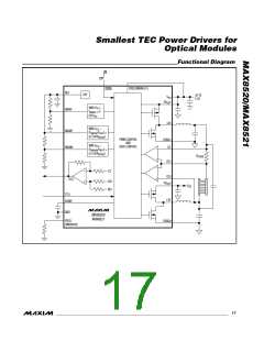
There are numerous ways to implement the thermal loop.
Figures 1 and 2 show designs that employ precision op
amps, along with a DAC or potentiometer to set the con-
trol temperature. The loop may also be implemented dig-
itally, using a precision A/D to read the thermistor or
other temperature sensor, a microcontroller to implement
the control algorithm, and a DAC (or filtered-PWM signal)
to send the appropriate signal to the MAX8520/MAX8521
CTLI input. Regardless of the form taken by the thermal-
control circuitry, all designs are similar in that they read
temperature, compare it to a set-point signal, and then
send an error-correcting signal to the MAX8520/
MAX8521 that moves the temperature in the appropriate
direction.
|V
- V
| = 4 x V
or V , whichever is lower
OS1
OS2
MAXV DD
Set V
with a resistor-divider between REF and
MAXV
GND using resistors from 10kΩ to 100kΩ. V
can
MAXV
vary from 0 to REF.
Control Inputs/Outputs
Output Current Control
The voltage at CTLI directly sets the TEC current. CTLI
is typically driven from the output of a temperature con-
trol loop. The transfer function relating current through
the TEC (I
) and V is given by:
CTLI
TEC
I
= (V
- V
) / (10 ✕ R )
REF SENSE
TEC
CTLI
where V
is 1.50V and:
REF
ITEC = (V
- V ) / R
CS SENSE
OS1
PC Board Layout and Routing
High switching frequencies and large peak currents
make PC board layout a very important part of design.
Good design minimizes excessive EMI and voltage
gradients in the ground plane, both of which can result
in instability or regulation errors. Follow these guide-
lines for good PC board layout:
CTLI is centered around REF (1.50V). I
CTLI = 1.50V. When V
from OS2 to OS1. The voltages on the pins relate as
follows:
is zero when
TEC
> 1.50V, the current flow is
CTLI
V
> V > V
OS1 CS
OS2
The opposite applies when V
from OS1 to OS2:
< 1.50V current flows
CTLI
1) Place decoupling capacitors as close to the IC pins
as possible.
V
< V < V
OS1 CS
OS2
2) Keep a separate power ground plane, which is con-
nected to PGND1 and PGND2. PV 1, PV 2,
DD
DD
Shutdown Control
PGND1, and PGND2 are noisy points. Connect
The MAX8520/MAX8521 can be placed in a power-saving
shutdown mode by driving SHDN low. When the
MAX8520/MAX8521 are shut down, the TEC is off (OS1
and OS2 decay to GND) and supply current is reduced to
2mA (typ).
decoupling capacitors from PV s to PGNDs as
DD
directly as possible. Output capacitors C2 and C7
returns are connected to PGND plane.
3) Connect a decoupling capacitor from V
to GND.
DD
Connect GND to a signal ground plane (separate
from the power ground plane above). Other V
decoupling capacitors (such as the input capacitor)
need to be connected to the PGND plane.
ITEC Output
DD
ITEC is a status output that provides a voltage proportional
to the actual TEC current. V
= REF when TEC current
is zero. The transfer function for the ITEC output is:
ITEC
4) Connect GND and PGND_ pins together at a single
point, as close as possible to the chip.
V
= 1.50 + 8 ✕ (V – V
)
CS
ITEC
OS1
Use ITEC to monitor the cooling or heating current
through the TEC. For stability, keep the load capaci-
tance on ITEC to less than 150pF.
5) Keep the power loop, which consists of input
capacitors, output inductors, and capacitors, as
compact and small as possible.
______________________________________________________________________________________ 15

 MAXIM [ MAXIM INTEGRATED PRODUCTS ]