NiCd /NiMH Ba t t e ry
Fa s t -Ch a rg e Co n t ro lle rs
ABSOLUTE MAXIMUM RATINGS
V+ to BATT-.................................................................-0.3V, +7V
BATT- to GND........................................................................±1V
BATT+ to BATT-
Power Not Applied ............................................................±20V
With Power Applied ................................The higher of ±20V or
±2V x (programmed cells)
REF Current.........................................................................10mA
Continuous Power Dissipation (T = +70°C)
A
Plastic DIP (derate 10.53mW/°C above +70°C............842mW
Narrow SO (derate 8.70mW/°C above +70°C .............696mW
CERDIP (derate 10.00mW/°C above +70°C ................800mW
Operating Temperature Ranges
DRV to GND ..............................................................-0.3V, +20V
FASTCHG to BATT-...................................................-0.3V, +12V
All Other Pins to GND......................................-0.3V, (V+ + 0.3V)
V+ Current.........................................................................100mA
DRV Current. .....................................................................100mA
MAX71_C_E .......................................................0°C to +70°C
MAX71_E_E .................................................... -40°C to +85°C
MAX71_MJE ................................................. -55°C to +125°C
Storage Temperature Range .............................-65°C to +150°C
Lead Temperature (soldering, 10sec) .............................+300°C
Stresses beyond those listed under “Absolute Maximum Ratings” may cause permanent damage to the device. These are stress ratings only, and functional
operation of the device at these or any other conditions beyond those indicated in the operational sections of the specifications is not implied. Exposure to
absolute maximum rating conditions for extended periods may affect device reliability.
2/MAX713
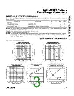
ELECTRICAL CHARACTERISTICS
(I = 10mA, T = T
to T , unless otherwise noted. Refer to Typical Operating Circuit. All measurements are with respect to
MAX
V+
A
MIN
BATT-, not GND.)
PARAMETER
CONDITIONS
MIN
4.5
5
TYP
MAX
UNITS
V
V+ Voltage
(Note 1)
5mA < I < 20mA
5.5
V+
I
V+
mA
µA
kΩ
µF
nF
V
BATT+ Leakage
V+ = 0V, BATT+ = 17V
5
BATT+ Resistance with Power On
C1 Capacitance
PGM0 = PGM1 = BATT-, BATT+ = 30V
30
0.5
5
C2 Capacitance
REF Voltage
0mA < I
Per cell
< 1mA
1.96
0.35
1.25
0
2.04
0.50
2.50
2
REF
Undervoltage Lockout
V
External VLIMIT Input Range
THI, TLO, TEMP Input Range
THI, TLO Offset Voltage (Note 2)
THI, TLO, TEMP, VLIMIT Input Bias Current
V
V
0V < TEMP < 2V, TEMP voltage rising
-10
-1
10
mV
µA
1
1.2V < V
PGM0 = PGM1 = V+
< 2.5V, 5mA < I
< 20mA,
LIMIT
DRV
VLIMIT Accuracy
-30
30
mV
Internal Cell Voltage Limit
Fast-Charge VSENSE
V
= V+
1.6
225
1.5
1.65
250
3.9
1.7
275
7.0
V
LIMIT
mV
PGM3 = V+
PGM3 = open
PGM3 = REF
PGM3 = BATT-
MAX713
4.5
7.8
12.0
20.0
38.0
Trickle-Charge VSENSE
mV
12.0
26.0
15.6
31.3
-2.5
0
mV/t
per cell
A
Voltage-Slope Sensitivity (Note 3)
Timer Accuracy
MAX712
-15
-1.5
30
15
%
Battery-Voltage to Cell-Voltage
Divider Accuracy
1.5
%
DRV Sink Current
V
DRV
= 10V
mA
2
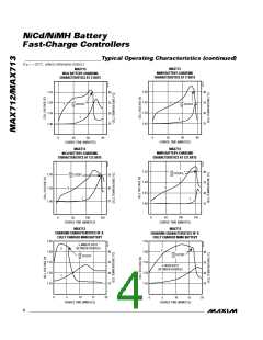
_______________________________________________________________________________________

 MAXIM [ MAXIM INTEGRATED PRODUCTS ]