Lo w -P o w e r, Du a l, 1 2 -Bit Vo lt a g e -Ou t p u t DACs
w it h S e ria l In t e rfa c e
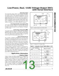
4/MAX15
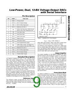
_____________________P in De s c rip t io n
OS_
R
PIN
1
NAME
AGND
OUTA
OSA
FUNCTION
Analog Ground
R
OUT_
2
DAC A Output Voltage
DAC A Offset Adjustment
Reference for DAC A
R
R
R
3
2R
D0
2R
D9
2R
D10
2R
D11
2R
4
REFA
Active-Low Clear Input. Resets all reg-
isters to zero. DAC outputs go to 0V.
5
CL
REF_
6
7
Chip-Select Input
Serial-Data Input
CS
AGND
DIN
SHOWN FOR ALL 1s ON DAC
8
SCLK
DGND
DOUT
UPO
Serial Clock Input
Digital Ground
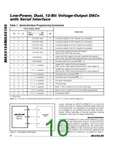
Figure 1. Simplified DAC Circuit Diagram
9
10
11
Serial-Data Output
User-Programmable Output
V
OUT
= (V
x NB / 4096) x 2
REF
where NB is the numeric value of the DAC’s binary input
code (0 to 4095) and V is the reference voltage.
REF
Power-Down Lockout. The device can-
not be powered down when PDL is low.
12
PDL
The reference input impedance ranges from 14kΩ (1554
hex) to several giga ohms (with an input code of 0000
hex). The reference input capacitance is code dependent
and typically ranges from 15pF with an input code of all
zeros to 50pF with a full-scale input code.
13
14
15
16
REFB
OSB
Reference for DAC B
DAC B Offset Adjustment
DAC B Output Voltage
Positive Power Supply
OUTB
Ou t p u t Am p lifie r
The output amplifiers on the MAX5154/MAX5155 have
internal resistors that provide for a gain of +2V/V when
OS_ is c onne c te d to AGND. The s e re s is tors a re
trimmed to minimize gain error. The output amplifiers
ha ve a typ ic a l s le w ra te of 0.75V/µs a nd s e ttle to
1/2LSB within 15µs, with a load of 10kΩ in parallel with
100pF. Loads less than 2kΩ degrade performance.
V
DD
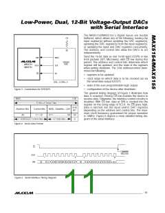
_______________De t a ile d De s c rip t io n
The MAX5154/MAX5155 dual, 12-bit, voltage-output
DACs are easily configured with a 3-wire serial inter-
face. These devices include a 16-bit data-in/data-out
shift register, and each DAC has a double-buffered
input composed of an input register and a DAC register
(see Functional Diagram). In addition, trimmed internal
resistors produce an internal gain of +2V/V that maxi-
mizes output voltage swing. The amplifier’s offset-adjust
pin allows for a DC shift in the DAC’s output.
The OS_ pin can be used to produce an adjustable off-
set voltage at the output. For instance, to achieve a 1V
offset, apply -1V to the OS_ pin to produce an output
range from 1V to (1V + V
output range is still limited by the maximum output volt-
age specification.
x 2). Note that the DAC’s
REF
Both DACs use an inverted R-2R ladder network that pro-
duces a weighted voltage proportional to the input volt-
age value. Each DAC has its own reference input to
facilitate independent full-scale values. Figure 1 depicts a
simplified circuit diagram of one of the two DACs.
P o w e r-Do w n Mo d e
The MAX5154/MAX5155 feature a software-program-
mable shutdown mode that reduces the typical supply
current to 2µA. The two DACs can be shutdown inde-
pendently, or simultaneously using the appropriate pro-
gramming command. Enter shutdown mode by writing
the appropriate input-control word (Table 1). In shut-
down mode, the reference inputs and amplifier out-
p uts b e c ome hig h imp e d a nc e , a nd the s e ria l
interface remains active. Data in the input registers is
Re fe re n c e In p u t s
The reference inputs accept both AC and DC values
with a voltage range extending from 0V to (V - 1.4V).
Determine the output voltage using the following equa-
tion (OS_ = AGND):
DD
_______________________________________________________________________________________
9

 MAXIM [ MAXIM INTEGRATED PRODUCTS ]