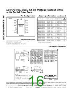
Lo w -P o w e r, Du a l, 1 2 -Bit Vo lt a g e -Ou t p u t DACs
w it h S e ria l In t e rfa c e
4/MAX15
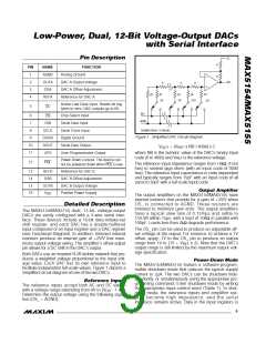
Serial-Data Output
OS_
+5V/+3V
The serial-data output, DOUT, is the internal shift regis-
ter’s output. DOUT allows for daisy chaining of devices
and data readback. The MAX5154/MAX5155 can be
p rog ra mme d to s hift d a ta out of DOUT on SCLK’s
falling edge (Mode 0) or on the rising edge (Mode 1).
Mode 0 provides a lag of 16 clock cycles, which main-
tains compatibility with SPI/QSPI and Microwire inter-
fa c e s . In Mod e 1, the outp ut d a ta la g s 15.5 c loc k
cycles. On power-up, the device defaults to Mode 0.
REF_
V
DD
R
R
MAX5154
MAX5155
DAC_
OUT_
AGND
DGND
User-Programmable Logic Output (UPO)
UPO allows an external device to be controlled through
the serial interface (Table 1), thereby reducing the
number of microcontroller I/O pins required. On power-
up, UPO is low.
GAIN = +2V/V
Figure 9. Unipolar Output Circuit (Rail-to-Rail)
Power-Down Lockout Input (PDL)
The power-down lockout pin (PDL) disables software
shutdown when low. When in shutdown, transitioning
PDL from high to low wakes up the part with the output
set to the state prior to shutdown. PDL can also be
used to asynchronously wake up the device.
OS_
+5V/+3V
REF_
V
OS
V
DD
R
R
MAX5154
MAX5155
Daisy Chaining Devices
Any numb e r of MAX5154/MAX5155s c a n b e d a is y
chained by connecting the DOUT pin of one device to
the DIN pin of the following device in the chain (Figure 7).
DAC _
OUT_
AGND
DGND
Since the MAX5154/MAX5155’s DOUT pin has an inter-
nal active pull-up, the DOUT sink/source capability
determines the time required to discharge/charge a
Figure 10. Setting OS_ for Output Offset
capacitive load. Refer to the digital output V and V
OH
OL
specifications in the Electrical Characteristics.
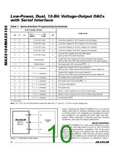
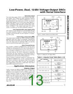
Table 2. Unipolar Code Table (Gain = +2)
Figure 8 shows an alternate method of connecting sev-
eral MAX5154/MAX5155s. In this configuration, the
data bus is common to all devices; data is not shifted
through a daisy chain. More I/O lines are required in
this configuration because a dedicated chip-select
input (CS) is required for each IC.
DAC CONTENTS
ANALOG OUTPUT
MSB
LSB
4095
4096
1 1 1 1 1 1 1 1 11 1 1 (0 )
1 0 0 0 0 0 0 0 00 0 1 (0 )
1 0 0 0 0 0 0 0 00 0 0 (0 )
0 1 1 1 1 1 1 1 11 1 1 (0 )
0 0 0 0 0 0 0 0 0 0 0 1 (0 )
+V
REF
x 2
x 2
=
__________Ap p lic a t io n s In fo rm a t io n
2049
4096
+V
REF
Un ip o la r Ou t p u t
Figure 9 shows the MAX5154/MAX5155 configured for
unipolar, rail-to-rail operation with a gain of +2V/V. The
MAX5154 c a n p rod uc e a 0V to 4.096V outp ut with
2.048V reference (Figure 9), while the MAX5155 can
produce a range of 0V to 2.5V with a 1.25V reference.
Table 2 lists the unipolar output codes. An offset to the
output can be achieved by connecting a voltage to
2048
4096
+V
REF
x 2
V
REF
2047
4096
+V
REF
x 2
1
+V
REF
x 2
OS_, as shown in Figure 10. By applying V _ = -1V,
OS
4096
the output values will range between 1V and (1V +
0 0 0 0 0 0 0 0 00 0 0 (0 )
0V
V
x 2).
REF
Note: ( ) are for the sub bit.
______________________________________________________________________________________ 13

 MAXIM [ MAXIM INTEGRATED PRODUCTS ]