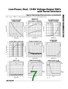
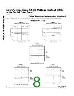
Lo w -P o w e r, Du a l, 1 2 -Bit Vo lt a g e -Ou t p u t DACs
w it h S e ria l In t e rfa c e
4/MAX15
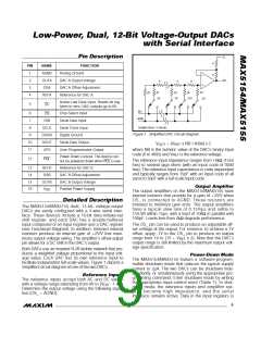
The MAX5154/MAX5155’s digital inputs are double
buffered, which allows any of the following: loading the
+5V
input register(s) without updating the DAC register(s),
updating the DAC register(s) from the input register(s),
or updating the input and DAC registers concurrently.
The address and control bits allow the DACs to act
SS
independently.
Send the 16-bit data as one 16-bit word (QSPI) or two
DIN
MOSI
SCK
8-bit packets (SPI, Microwire), with CS low during this
period. The address and control bits determine which
register will be updated, and the state of the registers
when exiting shutdown. The 3-bit address/control deter-
mines the following:
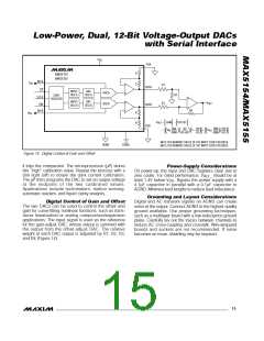
SPI/QSPI
PORT
MAX5154
MAX5155
SCLK
CS
I/O
•
•
registers to be updated
clock edge on which data is to be clocked out via
the serial-data output (DOUT)
CPOL = 0, CPHA = 0
•
•
state of the user-programmable logic output
configuration of the device after shutdown.
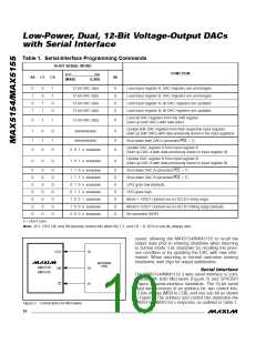
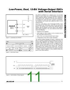
Figure 3. Connections for SPI/QSPI
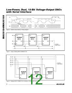
The general timing diagram of Figure 5 illustrates how
data is acquired. Driving CS low enables the device to
receive data. Otherwise, the interface control circuitry is
disabled. With CS low, data at DIN is clocked into the
register on the rising edge of SCLK. As CS goes high,
data is latched into the input and/or DAC registers
depending on the address and control bits. The maxi-
mum clock frequency guaranteed for proper operation
is 10MHz. Figure 6 depicts a more detailed timing dia-
gram of the serial interface.
MSB...................................................................................LSB
16 Bits of Serial Data
SUB
BIT
Address Bits
A0
Control Bits
MSB...DataBits...LSB
C1, C0
D11.......................D0
12 Data Bits
S0
0
1 Address/2 Control Bits
Figure 4. Serial-Data Format
CS
COMMAND
EXECUTED
SCLK
1
8
9
16
D5 D4 D3 D2 D1 D0 S0
C1
DIN
A0
C0 D11 D10 D9 D8 D7
D6
Figure 5. Serial-Interface Timing Diagram
______________________________________________________________________________________ 11

 MAXIM [ MAXIM INTEGRATED PRODUCTS ]