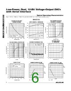
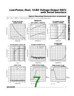
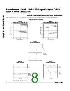
Lo w -P o w e r, Du a l, 1 2 -Bit Vo lt a g e -Ou t p u t DACs
w it h S e ria l In t e rfa c e
4/MAX15
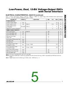
ELECTRICAL CHARACTERISTICS—MAX5155 (continued)
(V = +2.7V to +3.6V, V
= V
= 1.25V, R = 10kΩ, C = 100pF, T = T
to T
, unless otherwise noted. Typical values
MAX
DD
REFA
REFB
L
L
A
MIN
are at T = +25°C (OS_ pins tied to AGND for a gain of +2V/V).)
A
PARAMETER
POWER SUPPLIES
Positive Supply Voltage
Power-Supply Current
SYMBOL
CONDITIONS
MIN
TYP
MAX
UNITS
V
DD
2.7
3.6
0.6
V
I
DD
(Note 7)
(Note 7)
0.45
mA
Power-Supply Current
in Shutdown
I
1
0
8
µA
µA
DD (SHDN)
Reference Current in Shutdown
TIMING CHARACTERISTICS
SCLK Clock Period
±1
t
(Note 4)
100
40
ns
ns
ns
CP
SCLK Pulse Width High
SCLK Pulse Width Low
t
CH
t
40
CL
CS Fall to SCLK Rise
Setup Time
t
40
ns
CSS
t
0
50
0
ns
ns
ns
SCLK Rise to CS Rise Hold Time
SDI Setup Time
CSH
t
DS
SDI Hold Time
t
DH
SCLK Rise to DOUT Valid
Propagation Delay
t
C
C
= 200pF
= 200pF
120
120
ns
ns
DO1
DO2
LOAD
LOAD
SCLK Fall to DOUT Valid
Propagation Delay
t
t
10
40
ns
ns
ns
SCLK Rise to CS Fall Delay
CS Rise to SCLK Rise Hold
CS Pulse Width High
CS0
t
CS1
t
100
CSW
Note 5: Accuracy is specified from code 10 to code 4095.
Note 6: Accuracy is better than 1LSB for V greater than 6mV and less than V - 80mV. Guaranteed by PSRR test at the end
OUT
DD
points.
Note 7: Digital inputs are set to either V or DGND, code = 0000 hex, R = ∞.
DD
L
_______________________________________________________________________________________
5

 MAXIM [ MAXIM INTEGRATED PRODUCTS ]