Lo w -P o w e r, Du a l, 1 2 -Bit Vo lt a g e -Ou t p u t DACs
w it h S e ria l In t e rfa c e
4/MAX15
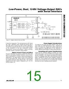
V
DD
OSA
R
R
MAX5154
MAX5155
REFA
V
IN
R1
R3
OUTA
OUTB
CS
INPUT
REG A
DAC
REG A
DACA
DACB
R2
SHIFT
REGISTER
SCLK
INPUT
REG B
DAC
REG B
V
OUT
DIN
R4
REFB
R
R
V
REF
V
OUT
= GAIN
–
OFFSET
[ ] [
]
OSB
2NA
R2
R4
1+
)( )( ) ( 2NB )(R4 )
=
V
V
REF
IN
(
[
R3 ] [
]
4096 R1+R2
4096 R3
NA IS THE NUMERIC VALUE OF THE INPUT CODE FOR DACA.
NB IS THE NUMERIC VALUE OF THE INPUT CODE FOR DACB.
AGND
DGND
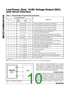
Figure 14. Digital Control of Gain and Offset
it trips the comparator. The microprocessor (µP) stores
this “high” calibration value. Repeat the process with a
dim light (off) to obtain the dark current calibration.
The µP then programs the DAC to set an output voltage
a t the mid p oint of the two c a lib ra te d va lue s .
Ap p lic a tions inc lud e ta c home te rs , motion s e ns ing ,
automatic readers, and liquid clarity analysis.
P o w e r-S u p p ly Co n s id e ra t io n s
On power-up, the input and DAC registers clear (set to
zero code). For rated performance, V should be at
REF_
least 1.4V below V . Bypass the power supply with a
DD
4.7µF capacitor in parallel with a 0.1µF capacitor to
AGND. Minimize lead lengths to reduce lead inductance.
Gro u n d in g a n d La yo u t Co n s id e ra t io n s
Digital and AC transient signals on AGND can create
noise at the output. Connect AGND to the highest quality
ground available. Use proper grounding techniques,
such as a multilayer board with a low-inductance ground
plane. Carefully lay out the traces between channels to
reduce AC cross-coupling and crosstalk. Wire-wrapped
boards and sockets are not recommended. If noise
becomes an issue, shielding may be required.
Dig it a l Co n t ro l o f Ga in a n d Offs e t
The two DACs can be used to control the offset and
gain for curve-fitting nonlinear functions, such as trans-
ducer linearization or analog compression/expansion
applications. The input signal is used as the reference
for the gain-adjust DAC, whose output is summed with
the output from the offset-adjust DAC. The relative
weight of each DAC output is adjusted by R1, R2, R3,
and R4 (Figure 14).
______________________________________________________________________________________ 15

 MAXIM [ MAXIM INTEGRATED PRODUCTS ]