5 V, Lo w -P o w e r, Vo lt a g e -Ou t p u t ,
S e ria l 1 0 -Bit DACs
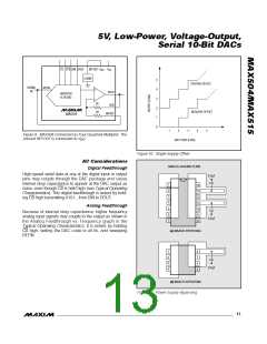
04/MAX15
code 0000.... REFIN’s input capacitance is also code
dependent and has a 50pF maximum value at several
codes.
R
S
REFOUT
TOTAL
REFERENCE
NOISE
C
S
If an upgrade to the internal reference is required, the 2.5V
C
REFOUT
MAX873A is suitable: ±15mV initial accuracy, TCV
7ppm/°C (max).
=
TEK 7A22
OUT
300
250
200
150
100
50
1.8
1.6
1.4
1.2
1.0
0.8
SINGLE POLE ROLLOFF
Logic Inte rfa c e
C
= 3.3µF
REFOUT
The MAX504/MAX515 logic inputs are designed to be
compatible with TTL or CMOS logic levels. However, to
achieve the lowest power dissipation, drive the digital
inputs with rail-to-rail CMOS logic. With TTL logic levels,
the power requirement increases by a factor of approxi-
mately 2.
0.6
0.4
0.2
0.0
C
= 47µF
REFOUT
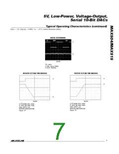
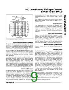
Serial Clock and Update Rate
Figure 1 shows the MAX504/MAX515 timing. The maxi-
0
mum serial clock rate is given by 1/(t +t ), approxi-
0.1
1
10
100
1000
CH CL
mately 14MHz. The digital update rate is limited by the
FREQUENCY (kHz)
chip-select period, which is 16 x (t
+ t ) + t
.
CH
CL
CSW
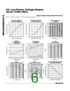
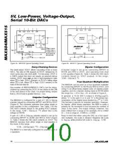
Figure 2. Reference Noise vs. Frequency
This equals a 1.14µs, or 877kHz, update rate. However,
the DAC settling time to 10 bits is 25µs, which may limit
the update rate to 40kHz for full-scale step transitions.
Inte rna l Re fe re nc e (MAX504 only)
The on-chip reference is laser trimmed to generate 2.048V
at REFOUT. The output stage can source and sink current
so REFOUT can settle to the correct voltage quickly in
response to code-dependent loading changes. Typically,
source current is 5mA and sink current is 100µA.
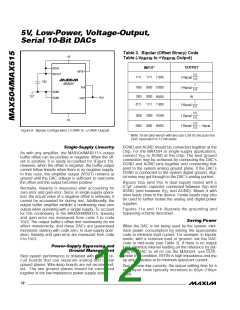
____________Applic a tions Inform a tion
Refer to Figures 3a and 3b for typical operating con-
nections.
Se ria l Inte rfa c e
REFOUT connects the internal reference to the R-2R DAC
ladder at REFIN. The R-2R ladder draws 50µA maximum
load current. If any other connection is made to REFOUT,
ensure that the total load current is less than 100µA to
avoid gain errors.
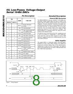
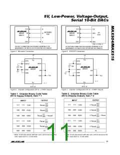
The MAX504/MAX515 use a three-wire serial interface that
is compatible with SPI™, QSPI™ (CPOL = CPHA = 0), and
Microwire™ standards as shown in Figures 4 and 5. The
DAC is programmed by writing two 8-bit words (see Figure
1 and the Functional Diagram). 16 bits of serial data are
clocked into the DAC in the following order: 4 fill (dummy)
bits, 10 data bits, and 2 sub-LSB 0s. The 4 dummy bits are
not normally needed, and are required only when DACs
are daisy chained. The 2 sub-LSB 0s, however, are always
needed, and allow hardware and software compatibility
with the 12-bit MAX531/MAX538/MAX539. Transitions at
CS should occur while SCLK is low. Data is clocked in on
SCLK’s rising edge while CS is low. The serial input data is
held in a 16-bit serial shift register. On CS’s rising edge, the
10 data-bits are transferred to the DAC register and update
the DAC. With CS high, data cannot be clocked into the
MAX504/MAX514.
For applications requiring very low-noise performance, con-
nect a 33µF capacitor from REFOUT to AGND. If noise is
not a concern, a lower value (3.3µF min) capacitor may be
used. To reduce noise further, insert a buffered RC filter
between REFOUT and REFIN (Figure 2). The reference
bypass capacitor C
is still required for reference sta-
REFOUT
bility. In applications not requiring the reference, connect
REFOUT to V (to save power and to eliminate the need
DD
for C
) or use the MAX515 (no internal reference).
REFOUT
Exte rna l Re fe re nc e
An external reference in the range (V + 2V) to (V - 2V)
SS
DD
may be used with the MAX504 in dual-supply operation.
With the MAX515 or the MAX504 in single-supply use, the
The MAX504/MAX515 inputs data in 16-bit blocks. The SPI
and Microwire interfaces output data in 8-bit blocks, there-
by requiring two write cycles to input data to the DAC. The
QSPI interface allows variable data input from 8 to 16 bits,
and can be loaded into the DAC in one write cycle.
reference must be positive and may not exceed V - 2V.
DD
The reference voltage determines the DAC’s full-scale out-
put. The DAC input resistance is code dependent and is
minimum (40kΩ) at code 0101... and virtually infinite at
SPI and QSPI are trademarks of Motorola, Inc. Microwire is a trademark of National Semiconductor Corp.
_______________________________________________________________________________________
9

 MAXIM [ MAXIM INTEGRATED PRODUCTS ]