5 V, Lo w -P o w e r, Vo lt a g e -Ou t p u t ,
S e ria l 1 0 -Bit DACs
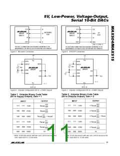
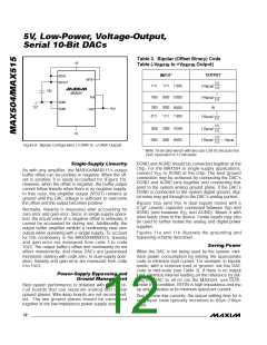
Table 3. Bipolar (Offset Binary) Code
Table (-V to +V Output)
+5V
REFIN
REFIN
OUTPUT
INPUT*
REFIN
BIPOFF
REFOUT
511
512
(+V
)
1111 1111
1000 0000
11(00)
01(00)
REFIN
33µF
MAX504
1
512
RFB
(+V
)
REFIN
AGND
DGND
1000 0000
0111 1111
00(00)
11(00)
0V
V
OUT
VOUT
1
512
(-V
)
)
REFIN
511
512
0000 0000
0000 0000
(-V
(-V
01(00)
00(00)
REFIN
04/MAX15
-5V
512
512
)
= -V
REFIN
REFIN
Figure 8. Bipolar Configuration (-2.048V to +2.048V Output)
* Write 10-bit data words with two sub-LSB 0s because the
DAC input latch is 12 bits wide.
DGND and AGND should be connected together at the
chip. For the MAX504 in single-supply applications,
S in g le -S u p p ly Lin e a rit y
As with any amplifier, the MAX504/MAX515’s output
buffer offset can be positive or negative. When the off-
set is positive, it is easily accounted for (Figure 10).
However, when the offset is negative, the buffer output
cannot follow linearly when there is no negative supply.
In that case, the amplifier output (VOUT) remains at
ground until the DAC voltage is sufficient to overcome
the offset and the output becomes positive.
connect V to AGND at the chip. The best ground
SS
connection may be achieved by connecting the DAC's
DGND and AGND pins together and connecting that
point to the system analog ground plane. If the DAC's
DGND is connected to the system digital ground, digi-
tal noise may get through to the DAC’s analog portion.
Bypass V
(and V in dual-supply mode) with a
SS
DD
0.1µF ceramic capacitor connected between V
and
DD
Normally, linearity is measured after accounting for
zero error and gain error. Since, in single-supply opera-
tion, the actual value of a negative offset is unknown, it
cannot be accounted for during test. Additionally, the
output buffer amplifier exhibits a nonlinearity near-zero
output when operating with a single supply. To account
for this nonlinearity in the MAX504/MAX515, linearity
a nd g a in e rror a re me a s ure d from c od e 3 to c od e
1023. The output buffer’s offset and nonlinearity do not
affect monotonicity, and these DACs are guaranteed
monotonic starting with code zero. In dual-supply oper-
ation, linearity and gain error are measured from code
0 to 1023.
AGND (and between V and AGND). Mount it with
SS
short leads close to the device. Ferrite beads may also
be used to further isolate the analog and digital power
supplies.
Fig ure s 11a a nd 11b illus tra te the g round ing a nd
bypassing scheme described.
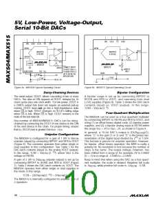
S a vin g P o w e r
When the DAC is not being used by the system, mini-
mize power consumption by setting the appropriate
code to minimize load current. For example, in bipolar
mode, with a resistive load to ground, set the DAC
code to mid-scale (see Table 3). If there is no output
load, minimize internal loading on the reference by set-
ting the DAC to a ll 0s (on the MAX504, us e CLR).
Under this condition, REFIN is high impedance and the
op amp operates at its minimum quiescent current.
P o w e r-S u p p ly Byp a s s in g a n d
Gro u n d Ma n a g e m e n t
Best system performance is obtained with printed cir-
c uit b oa rd s tha t us e s e p a ra te a na log a nd d ig ita l
ground planes. Wire-wrap boards are not recommend-
e d . The two g round p la ne s s hould b e c onne c te d
together at the low-impedance power-supply source.
Due to these low currents, the output settling time for a
zero input code typically increases to 60µs (100µs
max).
12 ______________________________________________________________________________________

 MAXIM [ MAXIM INTEGRATED PRODUCTS ]