5 V, Lo w -P o w e r, Vo lt a g e -Ou t p u t ,
S e ria l 1 0 -Bit DACs
DIN SCLK CS DOUT
DIN DOUT SCLK CS
REFIN
CLR
REFIN
VOUT
VOUT
INVERTED
R-2R DAC
INVERTED
R-2R DAC
REFOUT
2R
2R
2R
RFB
2.048V
MAX504
2R
CONNECT BIPOFF
TO VOUT FOR G=1,
TO AGND FOR G=2,
OR TO REFIN FOR
BIPOLAR GAIN
MAX515
BIPOFF
MAX515
ONLY
33µF
V
DD
V
AGND DGND
SS
AGND
V
DD
0.1µF
0.1µF
+5V
0V to -5V
0.1µF
+5V
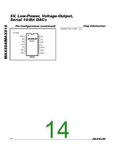
04/MAX15
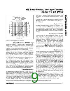
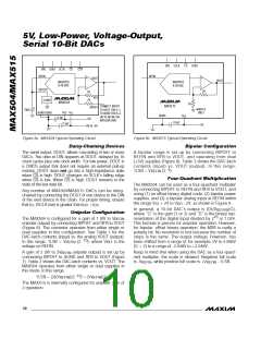
Figure 3a. MAX504 Typical Operating Circuit
Figure 3b. MAX515 Typical Operating Circuit
Da is y-Ch a in in g De vic e s
Bip o la r Co n fig u ra t io n
The serial output, DOUT, allows cascading of two or more
DACs. The data at DIN appears at DOUT, delayed by 16
clock cycles plus one clock width. For low power, DOUT is
a CMOS output that does not require an external pull-up
resistor. DOUT does not go into a high-impedance state
when CS is high. DOUT changes on SCLK’s falling edge
when CS is low. When CS is high, DOUT remains in the
state of the last data bit.
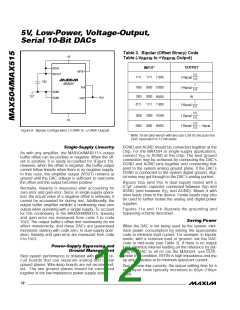
A bipolar range is set up by connecting BIPOFF to
REFIN a nd RFB to VOUT, a nd op e ra ting from d ua l
(±5V) supplies (Figure 8). Table 3 shows the DAC-latch
c onte nts (inp ut) vs . VOUT (outp ut). In this ra ng e ,
-9
1LSB = V
(2 ).
REFIN
Fo u r-Qu a d ra n t Mu lt ip lic a t io n
The MAX504 can be used as a four-quadrant multiplier
by connecting BIPOFF to REFIN and RFB to VOUT, and
using (1) an offset binary digital code, (2) bipolar power
supplies, and (3) a bipolar analog input at REFIN within
Any number of MAX504/MAX515 DACs can be daisy-
chained by connecting the DOUT of one device to the DIN
of the next device in the chain. For proper timing, ensure
the range V + 2V to V - 2V, as shown in Figure 9.
SS
DD
that t (SCLK low) is greater than t + t .
CL
DO
DS
In general, a 10-bit DAC’s output is (D)(V
(G),
REFIN)
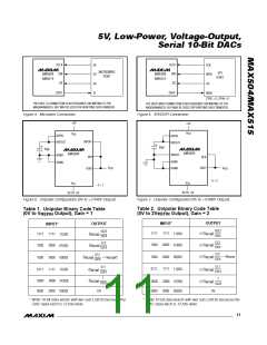
Un ip o la r Co n fig u ra t io n
The MAX504 is configured for a gain of 1 (0V to V
where “G” is the gain (1 or 2) and “D” is the binary rep-
10
resentation of the digital input divided by 2 or 1,024.
REFIN
unipolar output) by connecting BIPOFF and RFB to VOUT
(Figure 6). The converter operates from either single or
dual supplies in this configuration. See Table 1 for the
This formula is precise for unipolar operation. However,
for bipolar, offset binary operation, the MSB is really a
polarity bit. No resolution is lost because the number of
steps is the same. The output voltage, however, has
been shifted from a range of, for example, 0V to 4.096V
(G = 2) to a range of -2.048V to +2.048V.
DAC-latch contents (input) vs. the analog VOUT (output).
-10
In this range, 1LSB = V
(2
), where V
is the
REFIN
REF
voltage on REFIN.
A gain of 2 (0V to 2V
unipolar output) is set up by
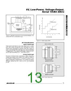
Keep in mind that when using the DAC as a four-quad-
rant multiplier, the scale is skewed. Negative full scale
REFIN
connecting BIPOFF to AGND and RFB to VOUT (Figure
7). Table 2 shows the DAC-latch contents vs. VOUT. The
MAX504 operates from either single or dual supplies in
this mode. In this range,
is -V
, while positive full scale is +V
- 1LSB.
REFIN
REFIN
-10
-9
1LSB = (2)(V )(2
REFIN
) = (V
)(2 ).
REFIN
The MAX515 is internally configured for unipolar gain of
2 operation.
10 ______________________________________________________________________________________

 MAXIM [ MAXIM INTEGRATED PRODUCTS ]