5 V, Lo w -P o w e r, Vo lt a g e -Ou t p u t
S e ria l 1 0 -Bit DACs
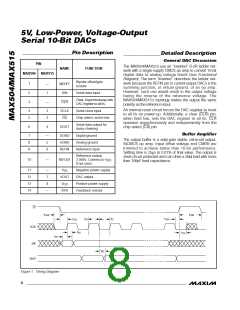
____________________P in De s c rip t io n
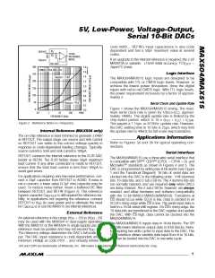
_______________De t a ile d De s c rip t io n
Ge n e ra l DAC Dis c u s s io n
PIN
The MAX504/MAX515 use an “inverted” R-2R ladder net-
work with a single-supply CMOS op amp to convert 10-bit
digital data to analog voltage levels (see Functional
Diagram). The term “inverted” describes the ladder net-
work because the REFIN pin in current-output DACs is the
summing junction, or virtual ground, of an op amp.
However, such use would result in the output voltage
b e ing the inve rs e of the re fe re nc e volta g e . The
MAX504/MAX515’s topology makes the output the same
polarity as the reference input.
NAME
FUNCTION
MAX504
MAX515
Bipolar offset/gain
resistor
—
1
BIPOFF
DIN
1
2
3
Serial data input
Clear. Asynchronously sets
DAC register to all 0s.
—
CLR
An internal reset circuit forces the DAC register to reset
to all 0s on power-up. Additionally, a clear (CLR) pin,
when held low, sets the DAC register to all 0s. CLR
operates asynchronously and independently from the
chip select (CS) pin.
4
5
2
3
SCLK
Serial clock input
Chip select, active low
CS
04/MAX15
Serial data output for
daisy-chaining
6
4
DOUT
Bu ffe r Am p lifie r
7
8
9
—
5
DGND
AGND
REFIN
Digital ground
The output buffer is a unity-gain stable, rail-to-rail output,
BiCMOS op amp. Input offset voltage and CMRR are
trimmed to achieve better than 10-bit performance.
Settling time is 25µs to 0.01% of final value. The output is
short-circuit protected and can drive a 2kΩ load with more
than 100pF load capacitance.
Analog ground
Reference input
Reference output,
2.048V. Connect to V
DD
if not used.
6
10
—
REFOUT
11
12
13
14
—
7
V
Negative power supply
DAC output
SS
VOUT
8
V
DD
Positive power supply
Feedback resistor
—
RFB
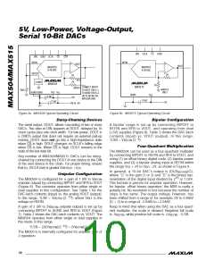
CS
t
t
CSH0
CSW
t
CH
t
t
CL
t
CSH1
CSS
SCLK
t
DH
t
CS1
t
DS
DIN
t
DO
DOUT
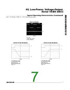
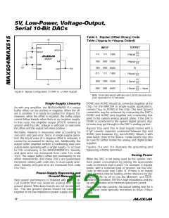
Figure 1. Timing Diagram
8
_______________________________________________________________________________________

 MAXIM [ MAXIM INTEGRATED PRODUCTS ]