±±5ꢀk EꢁDꢂ-rotected, HighꢂDrive Current, Dualꢂ/Quadꢂ/
OctalꢂLevel Translators with ꢁpeedꢂUp Circuitry
ABSOLUTE MAXIMUM RATINGS
ꢂAll voltages referenced to GNS.ꢃ
12-Pin TQFN ꢂderate 16.9mW/°C above +70°Cꢃ ........1349mW
12-ꢁump UCꢄP ꢂderate 6.5mW/°C above +70°Cꢃ ..... 519mW
20-Pin TQFN ꢂderate 20.8mW/°C above +70°Cꢃ ........1667mW
20-ꢁump UCꢄP ꢂderate 10.0mW/°C above +70°Cꢃ .....800mW
Operating Temperature Range ......................... -40°C to +85°C
ꢄtorage Temperature Range ........................... -65°C to +150°C
Junction Temperature .....................................................+150°C
ꢁump Temperature ꢂsolderingꢃ ...................................... +235°C
Lead Temperature ꢂsoldering, 10sꢃ ............................... +300°C
V
CC
......................................................................... -0.3V to +6V
V ............................................................................ -0.3V to +6V
L
I/O V
...................................................... -0.3V to V
+ 0.3V
CC_
CC
L
I/O V ........................................................... -0.3V to V + 0.3V
L_
EN ........................................................................... -0.3V to +6V
ꢄhort-Circuit Suration I/O V , I/O V to GNS ..... Continuous
L_
CC_
Maximum Continuous Current ........................................ 50mA
Continuous Power Sissipation ꢂT = +70°Cꢃ
A
8-Pin TSFN ꢂderate 18.2mW/°C above +70°Cꢃ ........ 1455mW
9-ꢁump UCꢄP ꢂderate 4.7mW/°C above +70°Cꢃ ........ 379mW
ꢄtresses beyond those listed under “Absolute Maximum Ratings” may cause permanent damage to the device. These are stress ratings only, and functional
operation of the device at these or any other conditions beyond those indicated in the operational sections of the specifications is not implied. Exposure to
absolute maximum rating conditions for extended periods may affect device reliability.
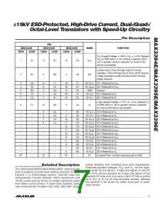
ELECTRICAL CHARACTERISTICS
ꢂV
CC
= +1.65V to +5.5V, V = +1.2V to V ; C
≤ 15pF, C ≤ 15pF; T = -40°C to +85°C, unless otherwise noted. Typical val-
IOVCC A
L
CC IOVL
ues are at T = +25°C.ꢃ ꢂNote 1ꢃ
A
PARAMETER
SYMBOL
CONDITIONS
MIN
TYP
MAX
UNITS
POWER SUPPLY
V ꢄupply Range
V
1.2
V
CC
V
V
L
L
V
ꢄupply Range
V
1.65
5.50
150
300
600
30
CC
CC
MAX3394E
MAX3395E
MAX3396E
MAX3394E
MAX3395E
MAX3396E
I/O lines internally
pulled up
ꢄupply Current from V
I
µA
µA
CC
L
CC
I/O lines internally
pulled up
ꢄupply Current from V
I
30
L
30
V
Tri-ꢄtate ꢄupply Current
I
EN = GNS, T = +25°C
3
6
µA
µA
CC
CC-3
A
45/MAX396E
V Tri-ꢄtate ꢄupply Current
L
I
EN = GNS, T = +25°C
0.7
2
L-3
A
LOGIC I/O
I/O V _ Input-Voltage ꢀigh
L
Threshold
0.7 x
V
L
V
V
IꢀL
I/O V _ Input-Voltage Low
L
Threshold
0.3 x
V
L
V
V
ILL
I/O V _ Internal Pullup SC
L
Resistance
R
EN = V
or V
L
5
10
15
10
20
kΩ
mA
mA
L
CC
I/O V _ ꢄource Current Suring
L
Low-to-ꢀigh Transition
I
V = +1.2V
L
IꢀL
I/O V _ ꢄink Current Suring ꢀigh-
L
to-Low Transition
I
V
= +1.65V
CC
ILL
2
_______________________________________________________________________________________

 MAXIM [ MAXIM INTEGRATED PRODUCTS ]