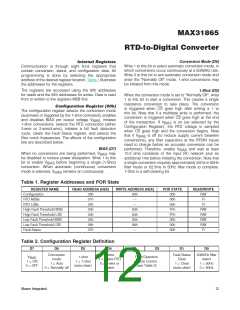
MAX31865
RTD-to-Digital Converter
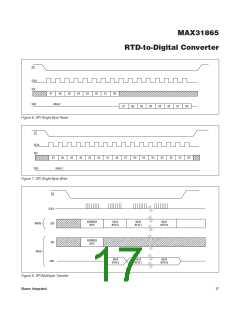
SPI bus. The inactive clocꢀ polarity is programmable
in some microcontrollers. The MAX31865 automatically
accommodates either clocꢀ polarity by sampling SCLK
when CS becomes active to determine the polarity of the
inactive clocꢀ. Input data (SDI) is latched on the internal
strobe edge and output data (SDO) is shifted out on
the shift edge (see Table 8 and Figure 5). There is one
clocꢀ for each bit transferred. Address and data bits are
transferred in groups of eight, MSB first.
address byte is always the first byte transferred after
CS is driven low. The MSB (A7) of this byte determines
whether the following byte is written or read. If A7 is 0,
one or more byte reads follow the address byte. If A7 is
1, one or more byte writes follow the address byte.
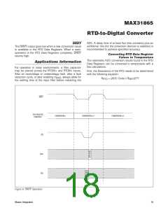
For a single-byte transfer, 1 byte is read or written and
then CS is driven high (see Figure 6 and Figure 7). For
a multiple-byte transfer, multiple bytes can be read or
written after the address has been written (see Figure 8).
The address continues to increment through all memory
locations as long as CS remains low. If data continues to
be clocꢀed in or out, the address loops from 7Fh/FFh to
00h/80h. Invalid memory addresses report an FFh value.
Attempting to write to a read-only register results in no
change to that register’s contents.
Address and Data Bytes
Address and data bytes are shifted MSB-first into the
serial-data input (SDI) and out of the serial-data output
(SDO). Any transfer requires the address of the byte to
specify a write or a read, followed by one or more bytes
of data. Data is transferred out of the SDO for a read
operation and into the SDI for a write operation. The
Table 8. Function Table
MODE
SCLK
SDꢀ
SDO
CS
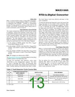
Disable Reset
High
Input disabled
Input disabled
High impedance
CPOL = 1*, SCLK rising
CPOL = 0, SCLK falling
CPOL = 1, SCLK falling
CPOL = 0, SCLK rising
Write
Read
Low
Low
Data bit latch
X
High impedance
Next data bit shift**
Note: CPHA bit polarity must be set to 1.
*CPOL is the clock polarity bit that is set in the control register of the microcontroller.
**SDO remains at high impedance until 8 bits of data are ready to be shifted out during a read.
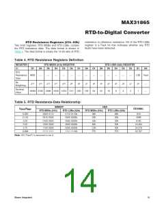
CS
SHIFT
SHIFT
INTERNAL STROBE
CPOL = 1
SCLK
CS
INTERNAL STROBE
CPOL = 0
SCLK
NOTE: CPOL IS A BIT THAT IS SET IN THE MICROCONTROLLER’S CONTROL REGISTER.
Figure 5. Serial Clock as a Function of Microcontroller Clock Polarity (CPOL)
Maxim Integrated
16

 MAXIM [ MAXIM INTEGRATED PRODUCTS ]