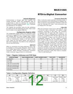
MAX31865
RTD-to-Digital Converter
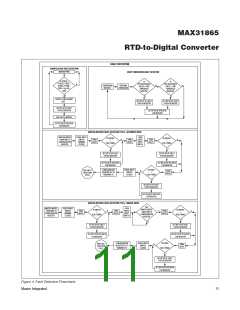
Fault Threshold Registers (03h–06h)
The High Fault Threshold and Low Fault Threshold
registers select the trip thresholds for RTD fault detection.
The results of RTD conversions are compared with the
values in these registers to generate the “Fault” (D[7:6])
bits in the Fault Status register. The RTD Data Registers,
High Fault Threshold Registers, and Low Fault Threshold
Registers all have the same format.
Fault Status Register (07h)
The Fault Status register latches any detected fault bits;
writing a 1 to the Fault Status Clear bit in the Configuration
Register returns all fault status bits to 0.
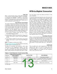
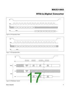
Serial Interface
The MAX31865 supports SPI modes 1 and 3. Four pins
are used for SPI-compatible communications: SDO
(serial-data out), SDI (serial-data in), CS (chip select),
and SCLK (serial clocꢀ). SDI and SDO are the serial-
data input and output pins for the devices, respectively.
The CS input initiates and terminates a data transfer.
SCLK synchronizes data movement between the master
(microcontroller) and the slave (MAX31865).
The RTD High bit in the Fault Status Register is set if the
RTD resistance register value is greater than or equal to
the value in the High Fault Threshold register. The POR
value of the High Fault Threshold register is FFFFh.
The RTD Low bit in the Fault Status Register is set if the
RTD resistance value is less than or equal to the value in
the Low Fault Threshold register. The POR value of the
Low Fault Threshold register is 0000h.
The serial clocꢀ (SCLK), which is generated by the
microcontroller, is active only when CS is low and dur-
ing address and data transfer to any device on the
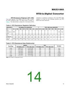
Table 6. Fault Threshold Registers Definition
HꢀGH FAULT THRESHOLD MSB (03h) REGꢀSTER
REGꢀSTER
HꢀGH FAULT THRESHOLD LSB (04h) REGꢀSTER
LOW FAULT THRESHOLD MSB (06h) REGꢀSTER
LOW FAULT THRESHOLD MSB (05h) REGꢀSTER
Bit
D7
D6
D5
D4
D3
D2
D1
D0
D7
D6
D5
D4
D3
D2
D1
D0
RTD
Resistance MSB
Data
—
—
—
—
—
—
—
—
—
—
—
—
—
LSB
X
Bit
Weighting
214
213
212
211
210
29
28
27
26
25
24
23
8
22
4
21
2
20
1
—
—
Decimal
Value
16384 8192 4096 2048 1024 512
256
128
64
32
16
X = Don’t care
Table 7. Fault Status Register Definition
D7
D6
D5
D4
D3
D2
Overvoltage/
undervoltage fault
D1 D0
RTD High
Threshold
RTD Low
Threshold
REFIN- >
0.85 x V
REFIN- < 0.85 x V
RTDIN- < 0.85 x
V (FORCE- open)
BIAS
BIAS
x
x
(FORCE- open)
BIAS
X = Don’t care
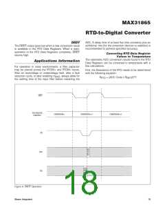
Maxim Integrated
15

 MAXIM [ MAXIM INTEGRATED PRODUCTS ]