Mu lt i-Ou t p u t , Lo w -No is e P o w e r-S u p p ly
Co n t ro lle rs fo r No t e b o o k Co m p u t e rs
0–MAX1635
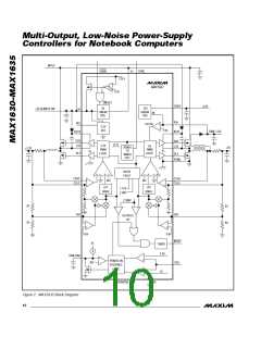
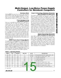
P WM Co n t ro lle r Blo c k
_______________De t a ile d De s c rip t io n
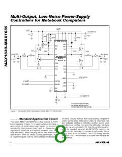
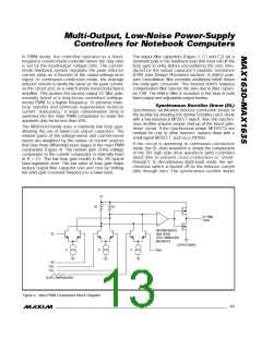
The two PWM controllers are nearly identical. The only
differences are fixed output settings (3.3V vs. 5V), the
VL/CSL5 bootstrap switch connected to the +5V PWM,
and SECFB. The heart of each current-mode PWM con-
troller is a multi-input, open-loop comparator that sums
thre e s ig na ls : the outp ut volta g e e rror s ig na l with
respect to the reference voltage, the current-sense sig-
nal, and the slope compensation ramp (Figure 3). The
PWM controller is a direct-summing type, lacking a tra-
ditional error amplifier and the phase shift associated
with it. This direct-summing configuration approaches
ideal cycle-by-cycle control over the output voltage.
The MAX1630 is a dual, BiCMOS, switch-mode power-
supply controller designed primarily for buck-topology
regulators in battery-powered applications where high effi-
ciency and low quiescent supply current are critical. Light-
load efficiency is enhanced by automatic Idle Mode™
operation, a variable-frequency pulse-skipping mode that
reduces transition and gate-charge losses. Each step-
down, power-switching circuit consists of two N-channel
MOSFETs, a rectifier, and an LC output filter. The output
voltage is the average AC voltage at the switching node,
which is regulated by changing the duty cycle of the
MOSFET switches. The gate-drive signal to the N-channel
high-side MOSFET must exceed the battery voltage, and
is provided by a flying-capacitor boost circuit that uses a
100nF capacitor connected to BST_.
When SKIP = low, Idle Mode circuitry automatically
optimizes efficiency throughout the load current range.
Idle Mode dramatically improves light-load efficiency
by reducing the effective frequency, which reduces
switching losses. It keeps the peak inductor current
above 25% of the full current limit in an active cycle,
allowing subsequent cycles to be skipped. Idle Mode
transitions seamlessly to fixed-frequency PWM opera-
tion as load current increases.
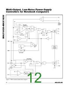
Devices in the MAX1630 family contain ten major circuit
blocks (Figure 2).
The two pulse-width modulation (PWM) controllers each
consist of a Dual Mode™ feedback network and multi-
plexer, a multi-input PWM comparator, high-side and
low-side gate drivers, and logic. MAX1630/MAX1631/
MAX1632 contain fault-protection circuits that monitor
the main PWM outputs for undervoltage and overvolt-
age. A power-on sequence block controls the power-
up timing of the main PWMs and determines whether
one or both of the outputs are monitored for undervolt-
a g e fa ults . The MAX1630/MAX1632/MAX1633/
MAX1635 include a secondary feedback network and
12V linear regulator to generate a 12V output from a
c oup le d -ind uc tor flyb a c k wind ing . The MAX1631/
MAX1634 have a secondary feedback input (SECFB)
instead, which allows a quasi-regulated, adjustable-
output, coupled-inductor flyback winding to be attached
to either the 3.3V or the 5V main inductor. Bias genera-
tor blocks include the 5V IC internal rail (VL) linear regu-
lator, 2.5V precision reference, and automatic bootstrap
s witc hove r c irc uit. The PWMs s ha re a c ommon
200kHz/300kHz synchronizable oscillator.
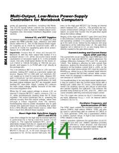
With SKIP = high, the controller always operates in
fixe d -fre q ue nc y PWM mod e for lowe s t nois e . Ea c h
pulse from the oscillator sets the main PWM latch that
turns on the high-side switch for a period determined
by the duty factor (approximately V /V ). As the
OUT IN
high-side switch turns off, the synchronous rectifier
latch sets; 60ns later, the low-side switch turns on. The
low-side switch stays on until the beginning of the next
clock cycle.
Table 3. SKIP PWM Table
LOAD
CURRENT
SKIP
MODE
DESCRIPTION
Pulse-skipping, supply cur-
rent = 250µA at V = 12V,
IN
discontinuous inductor
current
Low
Light
Idle
These internal IC blocks aren’t powered directly from
the battery. Instead, the 5V VL linear regulator steps
down the battery voltage to supply both VL and the
gate drivers. The synchronous-switch gate drivers are
directly powered from VL, while the high-side switch
gate drivers are indirectly powered from VL via an
external diode-capacitor boost circuit. An automatic
bootstrap circuit turns off the +5V linear regulator and
powers the IC from the 5V PWM output voltage if the
output is above 4.5V.
Constant-frequency PWM,
continuous inductor current
Low
High
High
Heavy
Light
PWM
PWM
PWM
Constant-frequency PWM,
continuous inductor current
Constant-frequency PWM,
continuous inductor current
Heavy
______________________________________________________________________________________ 11

 MAXIM [ MAXIM INTEGRATED PRODUCTS ]