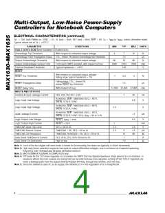
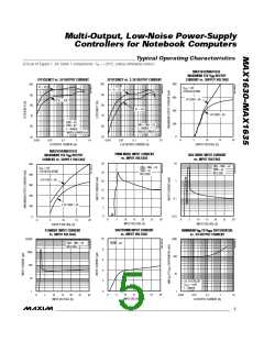
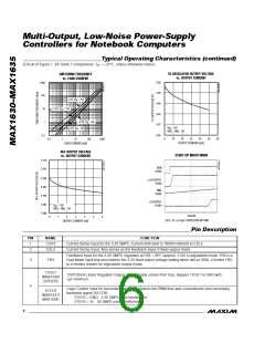
Mu lt i-Ou t p u t , Lo w -No is e P o w e r-S u p p ly
Co n t ro lle rs fo r No t e b o o k Co m p u t e rs
ON/OFF
INPUT
C3
+5V ALWAYS ON
4.7µF
10Ω
0.1µF
V+ SHDN SECFB VL
0.1µF
SYNC
BST3
4.7µF
0.1µF
BST5
DH5
Q3
Q4
Q1
Q2
DH3
LX3
DL3
0.1µF
L1
0.1µF
0.1µF
L2
R1
+5V OUTPUT
C1
R2
+3.3V OUTPUT
LX5
DL5
MAX1631
MAX1634
C2
*
*
PGND
6
CSH3
CSL3
FB3
CSH5
CSL5
FB5
RESET OUTPUT
RESET
TIME/ON5
RUN/ON3
5V ON/OFF
SKIP
3.3V ON/OFF
STEER
GND
REF
SEQ
+2.5V ALWAYS ON
1µF
*1A SCHOTTKY DIODE REQUIRED
FOR THE MAX1631 (SEE OUTPUT
OVERVOLTAGE PROTECTION SECTION).
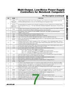
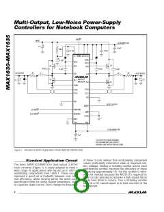
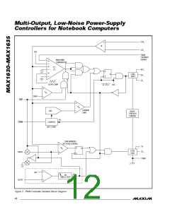
Figure 1. Standard 3.3V/5V Application Circuit (MAX1631/MAX1634)
of these circuits without first recalculating component
values (particularly inductance value at maximum bat-
tery voltage). Adding a Schottky rectifier across each
synchronous rectifier improves the efficiency of these
circuits by approximately 1%, but this rectifier is other-
wise not needed because the MOSFETs required for
these circuits typically incorporate a high-speed silicon
diode from drain to source. Use a Schottky rectifier
rated at a DC current equal to at least one-third of the
load current.
_______S t a n d a rd Ap p lic a t io n Circ u it
The b a s ic MAX1631/MAX1634 d ua l-outp ut 3.3V/5V
buck converter (Figure 1) is easily adapted to meet a
wide range of applications with inputs up to 28V by
substituting components from Table 1. These circuits
represent a good set of tradeoffs between cost, size,
a nd e ffic ie nc y, while s ta ying within the wors t-c a s e
specification limits for stress-related parameters, such
as capacitor ripple current. Don’t change the frequency
8
_______________________________________________________________________________________

 MAXIM [ MAXIM INTEGRATED PRODUCTS ]