Mu lt i-Ou t p u t , Lo w -No is e P o w e r-S u p p ly
Co n t ro lle rs fo r No t e b o o k Co m p u t e rs
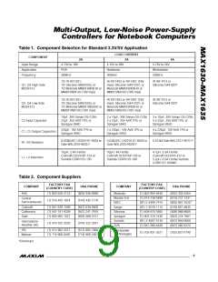
0–MAX1635
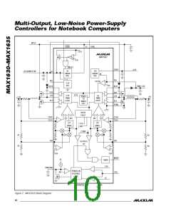
In PWM mod e , the c ontrolle r op e ra te s a s a fixe d -
The output filter capacitors (Figure 1, C1 and C2) set a
dominant pole in the feedback loop that must roll off the
loop gain to unity before encountering the zero intro-
duced by the output capacitor’s parasitic resistance
(ESR) (see Design Procedure section). A 60kHz pole-
zero cancellation filter provides additional rolloff above
the unity-gain crossover. This internal 60kHz lowpass
compensation filter cancels the zero due to filter capaci-
tor ESR. The 60kHz filter is included in the loop in both
fixed-output and adjustable-output modes.
frequency current-mode controller where the duty ratio
is set by the input/output voltage ratio. The current-
mode feedback system regulates the peak inductor
current value as a function of the output-voltage error
signal. In continuous-conduction mode, the average
inductor current is nearly the same as the peak current,
so the circuit acts as a switch-mode transconductance
amplifier. This pushes the second output LC filter pole,
normally found in a duty-factor-controlled (voltage-
mode) PWM, to a higher frequency. To preserve inner-
loop s ta b ility a nd e limina te re g e ne ra tive ind uc tor
current “staircasing,” a slope compensation ramp is
summed into the main PWM comparator to make the
apparent duty factor less than 50%.
S yn c h ro n o u s Re c t ifie r Drive r (DL)
Synchronous rectification reduces conduction losses in
the rectifier by shunting the normal Schottky catch diode
with a low-resistance MOSFET switch. Also, the synchro-
nous rectifier ensures proper start-up of the boost gate-
driver circuit. If the synchronous power MOSFETs are
omitted for cost or other reasons, replace them with a
small-signal MOSFET, such as a 2N7002.
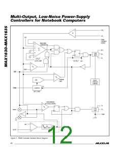
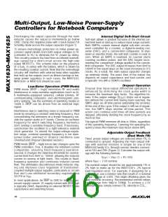
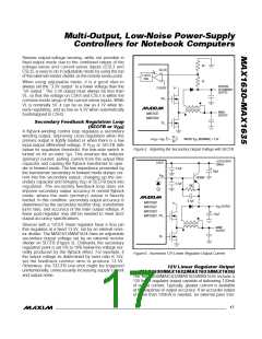
The MAX1630 family uses a relatively low loop gain,
allowing the use of lower-cost output capacitors. The
relative gains of the voltage-sense and current-sense
inputs are weighted by the values of current sources
that bias three differential input stages in the main PWM
comparator (Figure 4). The relative gain of the voltage
comparator to the current comparator is internally fixed
at K = 2:1. The low loop gain results in the 2% typical
load-regulation error. The low value of loop gain helps
reduce output filter capacitor size and cost by shifting
the unity-gain crossover frequency to a lower level.
If the c irc uit is ope ra ting in c ontinuous-c onduc tion
mode, the DL drive waveform is simply the complement
of the DH high-side drive waveform (with controlled
d e a d time to p re ve nt c ros s -c ond uc tion or “s hoot-
through”). In discontinuous (light-load) mode, the syn-
chronous switch is turned off as the inductor current
falls through zero. The synchronous rectifier works
VL
R1
R2
TO PWM
LOGIC
UNCOMPENSATED
HIGH-SPEED
FB_
LEVEL TRANSLATOR
AND BUFFER
OUTPUT DRIVER
I1
I2
I3
V
BIAS
REF
CSH_
CSL_
SLOPE COMPENSATION
Figure 4. Main PWM Comparator Block Diagram
______________________________________________________________________________________ 13

 MAXIM [ MAXIM INTEGRATED PRODUCTS ]