Mu lt i-Ou t p u t , Lo w -No is e P o w e r-S u p p ly
Co n t ro lle rs fo r No t e b o o k Co m p u t e rs
0–MAX1635
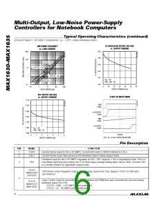
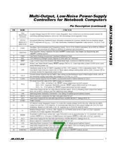
_________________________________________________P in De s c rip t io n (c o n t in u e d )
PIN
NAME
FUNCTION
V
DD
Supply Voltage Input for the 12OUT Linear Regulator. Also connects to an internal resistor divider for
secondary winding feedback, and to an 18V overvoltage shunt regulator clamp.
(MAX1630/
32/33/35)
5
SECFB
Secondary Winding Feedback Input. Normally connected to a resistor divider from an auxiliary output.
(MAX1631/
MAX1634)
SECFB regulates at V
used.
= 2.5V (see Secondary Feedback Regulation Loop section). Tie to VL if not
SECFB
Oscillator Synchronization and Frequency Select. Tie to VL for 300kHz operation; tie to GND for 200kHz
operation. Can be driven at 240kHz to 350kHz for external synchronization.
6
7
SYNC
Dual-Purpose Timing Capacitor Pin and ON/OFF Control Input. See Power-Up Sequencing and
ON/OFF Controls section.
TIME/ON5
8
9
GND
REF
Low-Noise Analog Ground and Feedback Reference Point
2.5V Reference Voltage Output. Bypass to GND with 1µF minimum.
Logic-Control Input that disables Idle Mode when high. Connect to GND for normal use.
10
SKIP
Active-Low Timed Reset Output. RESET swings GND to VL. Goes high after a fixed 32,000 clock-cycle
delay following power-up.
11
RESET
Feedback Input for the 5V SMPS; regulates at FB5 = REF (approx. 2.5V) in adjustable mode. FB5 is a
Dual Mode input that also selects the 5V fixed output voltage setting when tied to GND. Connect FB5 to
a resistor divider for adjustable-output mode.
12
FB5
Current-Sense Input for the 5V SMPS. Also serves as the feedback input in fixed-output mode, and as
the bootstrap supply input when the voltage on CSL5/VL is > 4.5V.
13
14
CSL5
CSH5
Current-Sense Input for the 5V SMPS. Current-limit level is 100mV referred to CSL5.
Pin-Strap Input that selects the SMPS power-up sequence:
SEQ = GND: 5V before 3.3V, RESET output determined by both outputs
SEQ = REF: Separate ON3/ON5 controls, RESET output determined by 3.3V output
SEQ = VL: 3.3V before 5V, RESET output determined by both outputs
15
SEQ
Gate-Drive Output for the 5V, high-side N-channel switch. DH5 is a floating driver output that swings
from LX5 to BST5, riding on the LX5 switching node voltage.
16
DH5
17
18
19
20
LX5
BST5
DL5
Switching Node (inductor) Connection. Can swing 2V below ground without hazard.
Boost capacitor connection for high-side gate drive (0.1µF)
Gate-Drive Output for the low-side synchronous-rectifier MOSFET. Swings 0V to VL.
Power Ground
PGND
5V Internal Linear-Regulator Output. VL is also the supply voltage rail for the chip. After the 5V SMPS
output has reached +4.5V (typical), VL automatically switches to the output voltage via CSL5 for boot-
strapping. Bypass to GND with 4.7µF. VL supplies up to 25mA for external loads.
21
VL
Battery Voltage Input, +4.2V to +30V. Bypass V+ to PGND close to the IC with a 0.22µF capacitor.
Connects to a linear regulator that powers VL.
22
23
V+
Shutdown Control Input, active low. Logic threshold is set at approximately 1V. For automatic start-up,
connect SHDN to V+ through a 220kΩ resistor and bypass SHDN to GND with a 0.01µF capacitor.
SHDN
24
25
26
DL3
BST3
LX3
Gate-Drive Output for the low-side synchronous-rectifier MOSFET. Swings 0V to VL.
Boost Capacitor Connection for high-side gate drive (0.1µF)
Switching Node (inductor) Connection. Can swing 2V below ground without hazard.
Gate-Drive Output for the 3.3V, high-side N-channel switch. DH3 is a floating driver output that swings
from LX3 to BST3, riding on the LX3 switching node voltage.
27
28
DH3
RUN/ON3
ON/OFF Control Input. See Power-Up Sequencing and ON/OFF Controls section.
_______________________________________________________________________________________
7

 MAXIM [ MAXIM INTEGRATED PRODUCTS ]