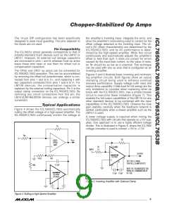
Chopper-Stabilized Op Amps
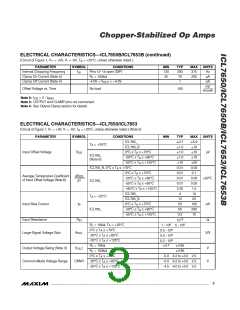
ELECTRICAL CHARACTERISTICS—ICL7650/ICL7653 (continued)
(Circuit of Figure 1, V+ = +5V, V- = -5V, T = +25°C, unless otherwise noted.) (Note 5)
A
PARAMETER
Common-Mode Rejection Ratio
Power-Supply Rejection Ratio
Input Noise Voltage
Input Noise Current
Unity-Gain Bandwidth
Slew Rate
SYMBOL
CMRR
CONDITIONS
CMVR = -5V to +2.5V
V+ to V- = 3V to 8V
MIN
120
120
TYP
130
130
2
MAX
UNITS
dB
PSRR
dB
e
np-p
R = 100Ω, f = 0 to 10Hz
S
µVp-p
pA/√Hz
MHz
V/µs
µs
I
n
f = 10Hz
0.01
2.0
2.5
0.2
20
GBW
SR
C = 50pF, R = 10kΩ
L
L
Rise Time
t
r
Overshoot
%
Operating Supply Range
Supply Current
V+ to V-
4.5
16
2.0
V
I
No load
1.2
200
70
1
mA
SUPP
Internal Chopping Frequency
Clamp On Current (Note 4)
Clamp Off Current (Note 4)
f
Pins 13 and 14 open (DIP)
R = 100kΩ
120
25
375
200
Hz
CLKOUT
µA
L
-4.0 ≤ V
≤ +4.0V
pA
OUT
nV/
√month
Offset Voltage vs. Time
100
Note 3: OUTPUT and CLAMP pins not connected.
Note 4: See Output Clamp section for details.
Note 5: All pins are designed to withstand electrostatic discharge (ESD) levels in excess of 2000V (MIL STD 8838 Method 3015.1
test circuit).
Note 6: Sample tested. Limits are not used to calculate outgoing quality level.
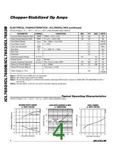
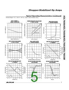
Typical Operating Characteristics
(Circuit of Figure 1, V+ = +5V, V- = -5V, T = +25°C, unless otherwise noted.)
A
MAXIMUM OUTPUT CURRENT
SUPPLY CURRENT
vs. SUPPLY VOLTAGE
CLOCK RIPPLE REFERRED TO INPUT
vs. SUPPLY VOLTAGE
vs. TEMPERATURE
4
3
1k
100
10
3
2
1
0
0.1µF
1µF
SOURCE CURRENT
2
1
BROADBAND
NOISE
0
(A = 1000)
V
-10
-20
-30
1
SINK CURRENT
0.1
2
4
6
8
10
12
14
16
25
50
75
100
125
150
4
6
8
10
12
14
16
TOTAL SUPPLY VOLTAGE (V)
TEMPERATURE (°C)
TOTAL SUPPLY VOLTAGE (V)
4
_______________________________________________________________________________________

 MAXIM [ MAXIM INTEGRATED PRODUCTS ]