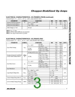
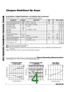
Chopper-Stabilized Op Amps
leakage at the null capacitor pins) becomes excessive
and 1µF external capacitors are required.
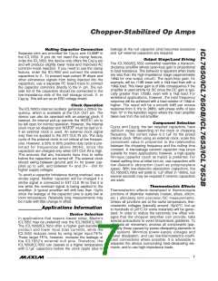
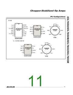
Nulling Capacitor Connection
Separate pins are provided for CRETN and CLAMP in
the ICL7650. If you do not need the clamp feature,
order the ICL7653; this device only offers the CRETN pin
and will produce slightly lower noise and improved AC
common-mode rejection. If you need to use the clamp
feature, order the ICL7650 and connect the external
capacitors to V-. To prevent load-current IR drops and
other extraneous signals from being injected into the
capacitors, use a separate PC board trace to connect
the capacitor commons directly to the V- pin. The out-
side foil of the capacitors should be connected to the
low-impedance side of the null storage circuit, V- or
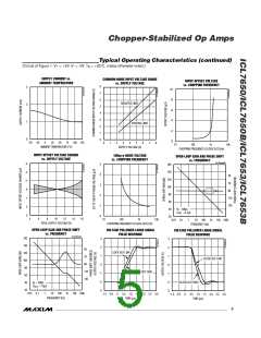
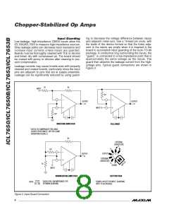
Output Stage/Load Driving
The ICL7650/ICL7653 somewhat resemble a transcon-
ductance amplifier whose open-loop gain is proportional
to load resistance. This behavior is apparent when loads
are less than the high-impedance stage (approximately
18kΩ for one output circuit). The open-loop gain, for
example, will be 17dB lower with a 1kΩ load than with a
10kΩ load. This lower gain is of little consequence if the
amplifier is used strictly for DC since the DC gain is typi-
cally greater than 120dB, even with a 1kΩ load. For
wideband applications, however, the best frequency
response will be achieved with a load resistor of 10kΩ or
higher. The result will be a smooth 6dB per octave
response from 0.1Hz to 2MHz, with phase shifts of less
than 10° in the transition region where the main amplifier
takes over from the null amplifier.
C
. This will act as an ESD voltage shield.
RETN
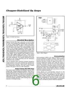
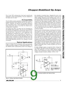
Clock Operation
The ICL7650’s internal oscillator generates a 200Hz fre-
quency, which is available at the CLK OUT pin. The
device can also be operated with an external clock, if
desired. An internal pull-up permits the INT/EXT pin to
be left open for normal operation. However, the internal
clock must be disabled and INT/EXT must be tied to V-
if an external clock is used. An external clock signal
may then be applied to the EXT CLK IN pin. The duty
cycle of the external clock is not critical at low frequen-
cies. However, a 50% to 80% positive duty cycle is pre-
ferred for frequencies above 500Hz, since the
capacitors are charged only when EXT CLK IN is high.
This ensures that any transients have time to settle
before the capacitors are turned off. The external clock
should swing between ground and V+ for power sup-
plies up to 6V, and between V+ and (V+ - 6V) for
higher supply voltages.
Component Selection
, the two required capacitors, have
EXTB
C
and C
EXTA
optimum values depending on the clock or chopping
frequency. The correct value is 0.1µF for the preset
internal clock. When using an external clock, scale this
component value in proportion to the relationship
between the chopping frequency and the nulling time
constant. A low-leakage ceramic capacitor may prove
suitable for many applications; however, a high-quality
film-type capacitor (such as mylar) is preferred. For
lowest settling time at initial turn-on, use capacitors with
low dielectric absorption (such as polypropylene
types). With low-dielectric-absorption capacitors, the
ICL7650/ICL7653 will settle to 1µV offset in 100ms, but
several seconds may be required if ceramic capacitors
are used.
To avoid a capacitor imbalance during overload, use a
strobe signal. Neither capacitor will be charged if a
strobe signal is connected to EXT CLK IN so that it is
low while the overload signal is being applied to the
amplifier. A typical amplifier will drift less than 10µVs
since the leakage of the capacitor pins is quite low at
room temperature. Relatively long measurements may
be made with little change in offset.
Thermoelectric Effects
Thermoelectric effects developed in thermocouple
junctions of dissimilar materials (metals, alloys, silicon,
etc.) ultimately limit precision DC measurements.
Unless all junctions are at the same temperature, ther-
moelectric voltages (typically around 10µV/°C, but up
to hundreds of µV/°C for some materials) will be gener-
ated. In order to realize the extremely low offset volt-
ages that the chopper amplifier can provide, take
special precautions to avoid temperature gradients. To
eliminate air movement, enclose all components (par-
ticularly those caused by power-dissipating elements in
the system). Minimize power-supply voltages and
power dissipation, and use low-thermoelectric-coeffi-
cient connections where possible. It is advisable to
separate the device surrounding heat-dissipating ele-
ments, and to use high-impedance loads.
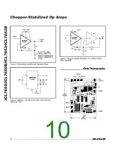
Applications Information
Device Selection
In applications that require lowest noise, Maxim’s
ICL7652 may be preferred over the ICL7650/ICL7653.
The ICL7650/ICL7653 offer a higher gain-bandwidth
product and lower input bias currents, while the
ICL7652 reduces noise by using larger input FETs.
These larger FETs, however, increase the leakage at
the ICL7652’s external null pins. Therefore, the
ICL7650/ICL7653 can operate to a higher temperature
with 0.1µF capacitors before the clock ripple (due to
_______________________________________________________________________________________
7

 MAXIM [ MAXIM INTEGRATED PRODUCTS ]