Chopper-Stabilized Op Amps
ing to decrease the voltage difference between inputs
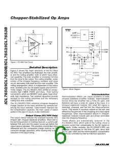
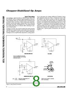
Input Guarding
Low-leakage, high-impedance CMOS inputs allow the
ICL7650/ICL7653 to measure high-impedance sources.
Stray leakage paths can decrease input resistance and
increase input currents unless inputs are guarded.
Boards must be thoroughly cleaned with TCE or alcohol
and blown dry with compressed air. The board should
be coated with epoxy or silicone after cleaning to pre-
vent contamination.
and adjacent metal runs. Use a 10-lead pin circle, with
the leads of the device formed so that the holes adja-
cent to the inputs are empty when it is inserted in the
board to accomplish input guarding of the 8-pin TO-99
package. A conductive ring surrounding the inputs, the
“guard,” is connected to a low-impedance point that is
approximately the same voltage as the inputs. The
guard then absorbs the leakage current from the high-
voltage pins. Typical guard connections are shown in
Figure 3.
Leakage currents may cause trouble even with properly
cleaned and coated boards, particularly since the input
pins are adjacent to pins that are at supply potentials.
Leakage can be significantly reduced by using guard-
R2
R1
INPUT
R3*
OUTPUT
OUTPUT
INPUT
R3*
INVERTING AMPLIFIER
FOLLOWER
*
USE R3 TO COMPENSATE FOR LARGE
SOURCE RESISTANCES, OR FOR CLAMP
OPERATION (FIGURE 5).
R2
EXTERNAL
CAPACITORS
V+
V-
R3*
OUTPUT
OUTPUT
7 8
4
1
6
5
2
EXTERNAL
CAPACITORS
3
R1
GUARD
INPUT
NONINVERTING AMPLIFIER
BOTTOM VIEW
R1 R2
SHOULD BE LOW IMPEDANCE FOR
R1 + R2 OPTIMUM GUARDING.
BOARD LAYOUT FOR INPUT GUARDING
WITH TO-99 PACKAGE.
NOTE:
Figure 3. Input Guard Connection
_______________________________________________________________________________________
8

 MAXIM [ MAXIM INTEGRATED PRODUCTS ]