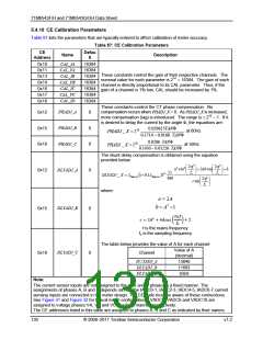
71M6543F/H and 71M6543G/GH Data Sheet
6.2
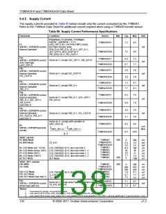
Recommended External Components
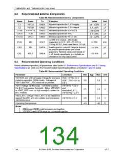
Table 89: Recommended External Components
To Function
Name
From
V3P3A
V3P3D
V3P3SYS
VDD
Value
Unit
µF
Bypass capacitor for 3.3 V supply
Bypass capacitor for 3.3 V output
Bypass capacitor for V3P3SYS
Bypass capacitor for VDD
C1
C2
GNDA
GNDD
GNDD
GNDD
GNDD
≥0.1 ±20%
0.1 ±20%
≥1.0 ±30%
0.1 ±20%
≥0.1 ±20%
µF
CSYS
CVDD
CVLCD
µF
µF
Bypass capacitor for VLCD pin
VLCD
µF
32.768 kHz crystal – electrically
XTAL
CXS
XIN
XIN
XOUT
GNDA
equivalent to ECS .327-12.5-17X or
Vishay XT26T, load capacitance 12.5 pF
32.768
kHz
pF
Load capacitor values for crystal depend
on crystal specifications and board
parasitics. Nominal values are based on
4 pF board capacitance and include an
allowance for chip capacitance.
15 ±10%
CXL
XOUT
GNDA
pF
10 ±10%
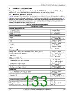
6.3
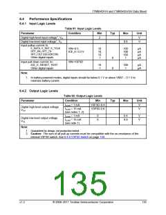
Recommended Operating Conditions
Unless otherwise specified, all parameters listed under 6.4 Performance Specifications and 6.5 Timing
Specifications are valid over the Recommended Operating Conditions provided in Table 90 below.
Table 90: Recommended Operating Conditions
Parameter
Condition
Min
Typ Max Unit
V3P3SYS and V3P3A Supply Voltage for precision VBAT=0 V to 3.8 V
metering operation (MSN mode). Voltages at
VBAT and VBAT_RTC need not be present.
3.0
3.6
V
VBAT_RTC =0 V to
3.8 V
VBAT Voltage (BRN mode). V3P3SYS is below
the 2.8 V comparator threshold. Either V3P3SYS
or VBAT_RTC must be high enough to power the
RTC module.
V3P3SYS < 2.8 V
and
Max(VBAT_RTC,
V3P3SYS) > 2.0 V
2.5
3.8
V
VBAT_RTC Voltage. VBAT_RTC is not needed to
support the RTC and non-volatile memory unless
V3P3SYS<2.0 V
V3P3SYS<2.0 V
2.0
-40
3.8
V
Operating Temperature
+85
ºC
Notes:
1. GNDA and GNDD must be connected together.
2. V3P3SYS and V3P3A must be connected together.
134
© 2008–2011 Teridian Semiconductor Corporation
v1.2

 MAXIM [ MAXIM INTEGRATED PRODUCTS ]