71M6543F/H and 71M6543G/GH Data Sheet
6
71M6543 Specifications
This section provides the electrical specifications for the 71M6543. Please refer to the 71M6xxx Data
Sheet for the 71M6xx3 electrical specifications, pin-out and package mechanical data.
6.1
Absolute Maximum Ratings
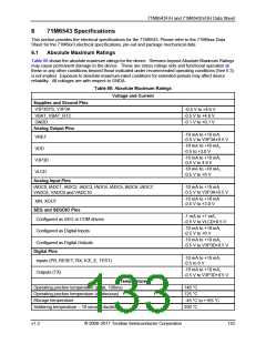
Table 88 shows the absolute maximum ratings for the device. Stresses beyond Absolute Maximum Ratings
may cause permanent damage to the device. These are stress ratings only and functional operation at
these or any other conditions beyond those indicated under recommended operating conditions (See 6.3)
is not implied. Exposure to absolute-maximum-rated conditions for extended periods may affect device
reliability. All voltages are with respect to GNDA.
Table 88: Absolute Maximum Ratings
Voltage and Current
Supplies and Ground Pins
V3P3SYS, V3P3A
VBAT, VBAT_RTC
GNDD
−0.5 V to +4.6 V
-0.5 V to +4.6 V
-0.1 V to +0.1 V
Analog Output Pins
-10 mA to +10 mA,
-0.5 V to V3P3A+0.5 V
VREF
VDD
-10 mA to +10 mA,
-0.5 to +3.0 V
-10 mA to +10 mA,
-0.5 V to 4.6 V
V3P3D
-10 mA to +10 mA,
-0.5 V to +6 V
VLCD
Analog Input Pins
IADC0, IADC1, IADC2, IADC3, IADC4, IADC5, IADC6, IADC7,
VADC8, VADC9 and VADC10
-10 mA to +10 mA
-0.5 V to V3P3A+0.5 V
-10 mA to +10 mA
-0.5 V to +3.0 V
XIN, XOUT
SEG and SEGDIO Pins
Configured as SEG or COM drivers
-1 mA to +1 mA,
-0.5 V to VLCD+0.5 V
-10 mA to +10 mA,
-0.5 V to +6 V
Configured as Digital Inputs
-10 mA to +10 mA,
-0.5 V to V3P3D+0.5 V
Configured as Digital Outputs
Digital Pins
-10 mA to +10 mA,
-0.5 to 6 V
Inputs (PB, RESET, RX, ICE_E, TEST)
-10 mA to +10 mA,
-0.5 V to V3P3D+0.5 V
Outputs (TX)
Temperature
Operating junction temperature (peak, 100ms)
Operating junction temperature (continuous)
Storage temperature
140 °C
125 °C
−45 °C to +165 °C
250 °C
Soldering temperature – 10 second duration
v1.2
© 2008–2011 Teridian Semiconductor Corporation
133

 MAXIM [ MAXIM INTEGRATED PRODUCTS ]