71M6543F/H and 71M6543G/GH Data Sheet
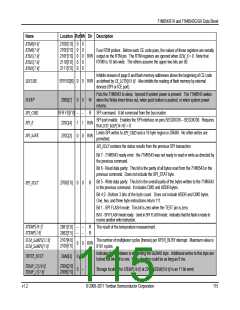
Name
Location Rst Wk Dir Description
LCD_SEG46[5:0]
to
LCD_SEG50[5:0]
243E[5:0]
to 2442[5:0]
0
0
–
–
R/W SEG data for SEG46 through SEG50. These pins cannot be configured as DIO.
LCD_SEGDIO51[5:0]
to
LCD_SEGDIO55[5:0]
2443[5:0] to
2447[5:0]
SEG and DIO data for SEGDIO51 through SEGDIO55. If configured as DIO, bit 1 is
R/W
direction (1 is output, 0 is input), bit 0 is data, and the other bits are ignored.
Specifies how VLCD is generated. See 2.5.10.3 for the definition of V3P3L.
Description
LCD_VMODE
11
10
01
00
External VLCD
LCD_VMODE[1:0]
2401[7:6] 00 00 R/W
LCD boost and LCD DAC enabled
LCD DAC enabled
No boost and no DAC. VLCD=V3P3L.
LCD Blink Frequency (ignored if blink is disabled).
1 = 1 Hz, 0 = 0.5 Hz
LCD_Y
2400[2]
2887[6:0]
2887[7]
0
0
0
0
–
0
0
0
R/W
LKPADDR[6:0]
LKPAUTOI
LKPDAT[7:0]
R/W The address for reading and writing the RTC lookup RAM.
Auto-increment flag. When set, LKPADDR[6:0] auto increments every time LKP_RD or
LKP_WR is pulsed. The incremented address can be read at LKPADDR.
R/W
2888[7:0]
R/W The data for reading and writing the RTC lookup RAM.
Strobe bits for the RTC lookup RAM read and write. When set, the LKPADDR[6:0] and
LKP_RD
LKP_WR
2889[1]
2889[0]
0
0
0
0
R/W
R/W
LKPDAT registers is used in a read or write operation. When a strobe is set, it stays set
until the operation completes, at which time the strobe is cleared and LKPADDR[6:0] is
incremented if LKPAUTOI is set.
MPU clock rate is:
[2:0])
MPU_DIV
MPU Rate = MCK Rate * 2-(2+
.
MPU_DIV[2:0]
2200[2:0]
0
0
R/W
The maximum value for MPU_DIV[2:0] is 4. Based on the default values of the PLL_FAST
bit and MPU_DIV[2:0], the power-up MPU rate is 6.29 MHz / 4 = 1.5725 MHz. The
minimum MPU clock rate is 38.4 kHz when PLL_FAST = 1.
MUX0_SEL[3:0]
MUX1_SEL[3:0]
MUX2_SEL[3:0]
MUX3_SEL[3:0]
MUX4_SEL[3:0]
MUX5_SEL[3:0]
MUX6_SEL[3:0]
MUX7_SEL[3:0]
2105[3:0]
2105[7:4]
2104[3:0]
2104[7:4]
2103[3:0]
2103[7:4]
2102[3:0]
2102[7:4]
0
0
0
0
0
0
0
0
0
0
0
0
0
0
0
0
R/W Selects which ADC input is to be converted during time slot 0.
R/W Selects which ADC input is to be converted during time slot 1.
R/W Selects which ADC input is to be converted during time slot 2.
R/W Selects which ADC input is to be converted during time slot 3.
R/W Selects which ADC input is to be converted during time slot 4.
R/W Selects which ADC input is to be converted during time slot 5.
R/W Selects which ADC input is to be converted during time slot 6.
R/W Selects which ADC input is to be converted during time slot 7.
v1.2
© 2008–2011 Teridian Semiconductor Corporation
111

 MAXIM [ MAXIM INTEGRATED PRODUCTS ]