250 mW Linear Power Amplifier and T/R Switch
AM55-0004
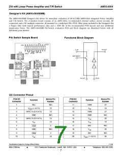
AM55-0004SMB Biasing Procedure
In order to prevent transients which may damage the MMIC, please adhere to the following procedure.
• Turn on all power supplies and set all voltages to 0 volts BEFORE connecting the power supplies to the
DC connector.
• Apply -4.0 volt supply or GND to DC connector pin 9 (VSW, see truth table for desired mode).
• Apply -4.0 volt supply or GND to DC connector pin 13 (VSW, see truth table for desired mode).
• Apply a -4.0 volt supply to the DC connector pin 16 (V ).
G1
• Apply a -4.0 volt supply to the DC connector pin 18 (V ).
G2
• Apply a +4.8 volt supply to the DC connector pin 2 (V ).
DD1
• Apply a +4.8 volt supply to the DC connector pin 20 (V ).
DD2
• Apply GND to DC connector pin 5 (Save Tx).
• Adjust V supply for desired V
quiescent current (typically 30 mA).
quiescent current (typically 65 mA).
G1
DD1
• Adjust V supply for desired V
G2
DD2
• Change voltage on DC connector pin 5 as required (Save Tx, see truth table for desired mode).
• Apply RF power and test.
• To power off, reverse above procedure
1. Set V & V to -4 V.
G1
G2
2. Set V
& V
to 0 V.
DD1
DD2
3. Set control voltage supplies to 0 V.
4. Disconnect bias lines from DC connector.
5. Turn off power supplies.
Evaluation PCB and RF Connector Losses
Port Reference
PA IN
Estimated Loss (dB)
0.15
0.20
0.20
0.20
0.20
PA OUT
Tx IN
ANT IN/OUT
Rx OUT
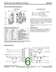
The DC connector on the Designer’s Kit PCB allows selection of all the device’s operating modes.
It is accomplished by one or more of the following methods:
1. A mating female multi-pin connector (Newark Electronics
Stock # 46F-4658, not included)
2. Wires soldered to the necessary pins (not included)
3. Clip leads (not included)
4. A combination of clip leads or wires and jumpers
(jumpers included as required)
Specifications Subject to Change Without Notice
V 2.00
M/A-COM Inc.
■
1011 Pawtucket Boulevard, Lowell, MA 01853 USA
■
Telephone: 800-366-2266
8

 TE [ TE CONNECTIVITY ]