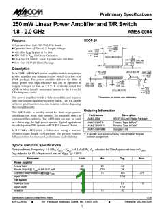
250 mW Linear Power Amplifier and T/R Switch
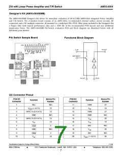
Designer’s Kit (AM55-0004SMB)
AM55-0004
The AM55-0004SMB Designer's Kit allows for immediate evaluation of M/A-COM's AM55-0004 integrated Power Amplifier
and T/R Switch. The evaluation board consists of an AM55-0004, recommended external surface mount circuitry, RF
connectors and a DC multipin connector, all mounted to a multi-layer FR-4 PCB. Other items included in the Designer's Kit:
a floppy disk (with typical performance data and a .DXF file of the recommended PCB layout) and any additional
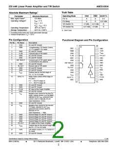
Application Notes. The AM55-0004SMB PA/Switch evaluation PCB and block diagram are illustrated below with all
functional ports labeled.
P/A Switch Sample Board
Functional Block Diagram
VG1
VDD2
VDD1
PA OUT
Tx IN
TX IN
VSW VG2
VSW
SAVE T
ANT IN/OUT
PA OUT
ANT IN/OUT
RX OUT
PA IN
Rx OUT
PA IN
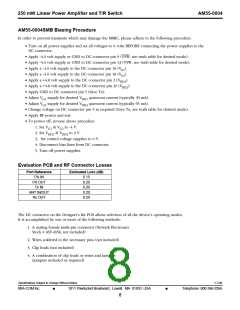
DC Connector Pinout
PCB DC
Connector
Device Pin
PCB DC
Connector
Device Pin
Number
Function
Function
Number
N/C
12
1
2
3
4
5
6
N/C
DD1 (+ 4.8 V)
11
12
13
14
15
16
VSW
VG1
27
18
V
SAVE Tx (0 V/-4 V)
GND
13
VSW
GND
VG2
27
N/C
13
N/C
20
SAVE Tx (0 V/-4 V)
VG1
18
VG1
18
7
8
2
17
18
N/C
VG2
N/C
20
VSW
GND
N/C
9
2
19
20
N/C
N/C
26
VSW
VG1
10
18
VDD2 ( + 4.8 V)
Specifications Subject to Change Without Notice
V 2.00
M/A-COM Inc.
■
1011 Pawtucket Boulevard, Lowell, MA 01853 USA
■
Telephone: 800-366-2266
7

 TE [ TE CONNECTIVITY ]