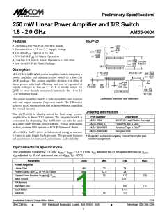
250 mW Linear Power Amplifier and T/R Switch
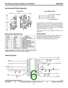
Recommended PCB Configuration
AM55-0004
Layout View
Cross-Section View
0.700 in.
RF Traces + Components
C1
C6
Pin 1
RF Ground
DC Routing
C9
Customer Defined
C10
R3 C2 R2
0.490 in.
R1
The PCB dielectric between RF traces and RF ground layers
should be chosen to reduce RF discontinuities between
50-Ω lines and package pins. M/A-COM recommends an
FR-4 dielectric thickness of 0.008 in. (0.2 mm), yielding a
50-Ω line width of 0.015 in. (0.38 mm). The recommended
metalization thickness is 1 oz. copper.
C5
C3
C8
C7
C4
Shaded traces are vias to DC routing layer and traces on DC
routing layer.
Biasing Procedure
External Circuitry Parts List
The AM55-0004 requires that VGG bias be applied prior to
any VDD bias. Permanent damage may occur if this
procedure is not followed. All FETs in the PA will draw
excessive current and damage internal circuitry.
Label
C1 - C5
C6 - C8
C9
Value
1000 pF
68 pF
Purpose
Low frequency bypass
RF bypass
1.5 pF
Output power tuning
Reduces low frequency gain
Voltage divider to VG2
Voltage divider to VG2
Reduces low frequency gain
Power match
C10
15 pF
R1
2.7 k Ω
1.5 k Ω
150 Ω
R2
R3
Tline
0.250 in. long
All off-chip components are low-cost surface mount components obtainable from
multiple sources. (0.020 in. x 0.040 in. or 0.030 in. x 0.050 in.)
External Circuitry
VSW
VDD2
1
2
28
27
26
25
24
23
22
21
20
19
18
17
16
15
C1
C6
VSW
Tx IN
3
4
TLine
PA OUT
C9
5
6
7
C10
R3
ANT IN/OUT
R1
8
Rx OUT
VDD1
VG2
9
C2
10
11
12
13
14
R2
C8
C5
VG1
C3
C7
Save Tx
C4
PA IN
Specifications Subject to Change Without Notice
V 2.00
M/A-COM Inc.
■
1011 Pawtucket Boulevard, Lowell, MA 01853 USA
■
Telephone: 800-366-2266
6

 TE [ TE CONNECTIVITY ]