250 mW Linear Power Amplifier and T/R Switch
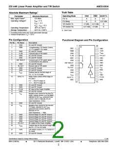
Absolute Maximum Ratings1
AM55-0004
Truth Table
Operating Mode
PA Tx
VSW
X
VSW
SAVE Tx
Parameter
Max. Input Power2
Operating Voltages2
Absolute Maximum
+23 dBm
VDD = 7 V
X
X
0 V
PA Sleep
X
-4.0 Volts
VGG = -5 V
T/R Switch Tx
T/R Switch Rx
0 Volts -4.0 Volts
-4.0 Volts 0 Volts
X
X
VDD - VGG = 8 V
Operating Temperature
Storage Temperature
-40°C to +85°C
-65°C to +150°C
X - Don’t Care
1. Exceeding these limits may cause permanent damage.
2. Ambient temperature (T ) = +25°C
A
Pin Configuration
Pin No. Pin Name
Functional Diagram and Pin Configuration
Description
1
2
GND
VSW
DC and RF Ground
1
28
Complimentary T/R Switch Control,
-4 V Tx mode/0 V Rx mode
GND
GND
VSW
V
VDDDD12
VSW
GND
Tx IN
GND
GND
3
4
5
6
7
GND
Tx IN
DC and RF Ground
Transmit side of T/R switch
DC and RF Ground
DC and RF Ground
GND
PA OUT
GND
GND
ANT IN/OUT
Common port of T/R switch which
is connected to the antenna
GND
GND
ANT IN/OUT
GND
8
GND
Rx OUT
GND
GND
V
DC and RF Ground
GND
V
VGG12
9
Receive side of T/R switch
DC and RF Ground
Rx OUT
10
11
12
GND
V
GND
GND
DC and RF Ground
Positive bias for the first stage of
PA, +2.7 to +6.0 volts
Sleep mode control of first stage of
PA ONLY
VG1
1
DD
G2
VDD1
GND
PA IN
GND
13
SAVE Tx
SAVE Tx
GND
0 V — first PA stage on
-4 V — first PA stage off
DC and RF Ground
14
15
14
15
16
17
18
GND
GND
PA IN
GND
DC and RF Ground
RF input of the Power Amplifier
DC and RF Ground
V
Negative bias control for the first PA
stage, voltage divider is on the MMIC,
G1
adjusted to set V
quiescent bias
DD1
current, which is typically 30 mA.
Input impedance: 10 kΩ
19
20
GND
DC and RF Ground
V
Negative bias control for the second
PA stage, adjusted to set V
G2
DD2
quiescent bias current, which is
typically 65 mA.
Input impedance: > 1MΩ
21
22
23
24
25
26
GND
GND
Second Stage DC and RF Ground
Second Stage DC and RF Ground
Second Stage DC and RF Ground
Second Stage DC and RF Ground
RF output of the Power Amplifier
GND
GND
PA OUT
V
Positive bias for the second stage of
the PA, +2.7 to +6.0 volts
DD2
27
28
VSW
GND
T/R Switch Control, 0 V Tx mode/-4 V
Rx mode
DC and RF Ground
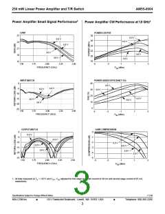
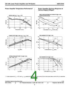
Specifications Subject to Change Without Notice
V 2.00
M/A-COM Inc.
■
1011 Pawtucket Boulevard, Lowell, MA 01853 USA
■
Telephone: 800-366-2266
2

 TE [ TE CONNECTIVITY ]